SPICE It up: How to Extract the Input Capacitance of an Op Amp (Part 3)
In operational amplifier (op amp) applications, the feedback resistance of the amplifier interacts with its input capacitance to create a zero in the noise-gain response of the amplifier. This zero in the response, unless properly compensated, reduces the amplifier’s phase margin, causing a peaked frequency response with possible instability – or at the very least ringing in the pulse response.
The amplifier’s input capacitance may be the dominant source capacitance in high-speed transimpedance applications where avalanche photo diodes (APDs) serve as the front-end sensor. An accurate model of the input capacitance is vitally important in such situations to ensure that the simulations closely match bench measurements. Op-amp macro-models with inaccurate input capacitances will result to erroneous simulation results.
In this blog post, I will explore methods to extract the common-mode and differential input capacitance of an amplifier. Figure 1 shows an example of an op amp circuit with the configuration of the internal capacitances explicitly drawn. The differential input capacitance has a minor effect on loop gain, since the amplifier’s closed-loop, virtual-ground behavior bootstraps the input terminals together, thereby lowering the effect of the differential capacitance. The printed circuit board (PCB) parasitic capacitance on the inverting input pin will also affect the loop-gain response and hence its stability. You must take care during layout to minimize this parasitic capacitance.
 Figure 1 Op-amp Model Showing Input
Common-mode and Differential Capacitance
Figure 1 Op-amp Model Showing Input
Common-mode and Differential CapacitanceTo model the input capacitance of the amplifier, I used an op-amp model without internal input capacitances and added external capacitors. Table 1 lists the amplifier specifications I used.

|
I used different values of common-mode capacitances (inverting and noninverting) for the purposes of illustration. In most op amps, the common-mode capacitance on the inverting and noninverting inputs will be equal; however, current-feedback amplifiers (CFAs) are an exception to this rule.
Figure 2 shows the TINA-TI™ software schematic and Figure 3 shows the simulated closed-loop response of the amplifier.
 Figure 2 TINA-TI Software Schematic of
an Op-amp Buffer
Figure 2 TINA-TI Software Schematic of
an Op-amp Buffer Figure 3 Closed-loop Bandwidth of a
Buffer
Figure 3 Closed-loop Bandwidth of a
BufferNoninverting Node Capacitance (CCM+)
In order to extract CCM+, add a series resistance at the input of the noninverting pin (as shown in Figure 4) and measure the frequency response at the noninverting node. The series resistor forms a low-pass filter (LPF) whose cutoff frequency is a function of the resistor and the internal capacitance. Select a value of resistance such that the -3dB LPF cutoff frequency is much less than the closed-loop bandwidth of the amplifier to ensure that the amplifier is in its linear operating region. You cannot make the value of resistance arbitrarily large. The voltage drop across resistor R1 is due to the bias current and may violate the amplifier’s input common-mode and/or output-swing specifications. Alternatively, you can use an inductor instead of a series resistor to create the LPF. The extracted capacitance, from the simulated frequency response, is:

The simulated response of the amplifier measured at its non-inverting input is shown in Figure 5.
 Figure 4 TINA-TI Software Schematic
CCM+
Figure 4 TINA-TI Software Schematic
CCM+ Figure 5 Simulated Response for
CCM+ Extraction
Figure 5 Simulated Response for
CCM+ ExtractionInverting Node Capacitance (CCM-)
In order to extract CCM-, add a feedback resistor (R1) to the buffer configuration. CCM- and R1 create a zero in the noise-gain curve. The zero in the noise-gain curve peaks the amplifier’s frequency response. Choose the value of R1 carefully so that the location of the zero is much lower than the closed-loop gain of the amplifier to prevent its open-loop gain limitations from affecting your calculations. Figure 6 and Figure 7 show the circuit for this test and the results, respectively. The extracted capacitance, from the simulated frequency response, is:

 Figure 6 TINA-TI Software Schematic
CCM-
Figure 6 TINA-TI Software Schematic
CCM- Figure 7 Simulated Response for
CCM- Extraction
Figure 7 Simulated Response for
CCM- ExtractionDifferential Capacitance (CDIFF)
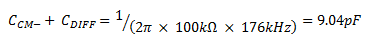
Measuring CDIFF is a little more complicated, as the virtual ground of the amplifier forces its input nodes to track each other – thus bootstrapping the capacitor’s terminals. Figure 8 shows the circuit used to measure CDIFF. The amplifier is in an inverting configuration at DC; however, the feedback inductor puts the amplifier in an open-loop configuration at higher frequencies. The input resistor R1 and the parallel combination of CCM- and CDIFF form a low-pass filter, whose corner frequency is measured by probing the amplifier’s inverting terminal. The extracted capacitance, from the simulated frequency response, is thus:
The simulated frequency response of the circuit in Figure 8 is shown in Figure 9.
 Figure 8 TINA-TI Software Schematic
CDIFF
Figure 8 TINA-TI Software Schematic
CDIFF Figure 9 Simulated Response for
CDIFF Extraction
Figure 9 Simulated Response for
CDIFF ExtractionIn cases where the capacitance modeled is larger than the specified data sheet value, TINA-TI software allows the use of a negative capacitor to correct the modeled value.
I have covered some of the methods for extracting the common-mode and differential input capacitance of an amplifier; however, these are not the only ways. In what ways have you extracted an amplifier’s common-mode and differential input capacitance? Please log in to your TI E2E™ Community account and leave a comment below so we can start a discussion.
Additional Resources
- Learn more about TI’s high-speed amplifier portfolio and find more technical resources.
- Get started on your design with Amplifier Product SelGuide software.
- Join the conversation on the TI E2E Community High Speed Amplifiers forum.
- Search TI high-speed op amps and find technical resources.
IMPORTANT NOTICE AND DISCLAIMER
TI PROVIDES TECHNICAL AND RELIABILITY DATA (INCLUDING DATASHEETS), DESIGN RESOURCES (INCLUDING REFERENCE DESIGNS), APPLICATION OR OTHER DESIGN ADVICE, WEB TOOLS, SAFETY INFORMATION, AND OTHER RESOURCES “AS IS” AND WITH ALL FAULTS, AND DISCLAIMS ALL WARRANTIES, EXPRESS AND IMPLIED, INCLUDING WITHOUT LIMITATION ANY IMPLIED WARRANTIES OF MERCHANTABILITY, FITNESS FOR A PARTICULAR PURPOSE OR NON-INFRINGEMENT OF THIRD PARTY INTELLECTUAL PROPERTY RIGHTS.
These resources are intended for skilled developers designing with TI products. You are solely responsible for (1) selecting the appropriate TI products for your application, (2) designing, validating and testing your application, and (3) ensuring your application meets applicable standards, and any other safety, security, or other requirements. These resources are subject to change without notice. TI grants you permission to use these resources only for development of an application that uses the TI products described in the resource. Other reproduction and display of these resources is prohibited. No license is granted to any other TI intellectual property right or to any third party intellectual property right. TI disclaims responsibility for, and you will fully indemnify TI and its representatives against, any claims, damages, costs, losses, and liabilities arising out of your use of these resources.
TI’s products are provided subject to TI’s Terms of Sale (www.ti.com/legal/termsofsale.html) or other applicable terms available either on ti.com or provided in conjunction with such TI products. TI’s provision of these resources does not expand or otherwise alter TI’s applicable warranties or warranty disclaimers for TI products.
Mailing Address: Texas Instruments, Post Office Box 655303, Dallas, Texas 75265
Copyright © 2023, Texas Instruments Incorporated