SWRS121E July 2012 – January 2016 CC2560 , CC2560B , CC2564
PRODUCTION DATA.
- 1Device Overview
- 2Revision History
- 3Device Comparison
- 4Terminal Configuration and Functions
-
5Specifications
- 5.1 Absolute Maximum Ratings
- 5.2 Recommended Operating Conditions
- 5.3 Power Consumption Summary
- 5.4 Electrical Characteristics
- 5.5
Timing and Switching Characteristics
- 5.5.1 Device Power Supply
- 5.5.2 Clock Specifications
- 5.5.3 Peripherals
- 5.5.4
RF Performance
- 5.5.4.1
Bluetooth BR/EDR RF Performance
- 5.5.4.1.1 Bluetooth Receiver—In-Band Signals
- 5.5.4.1.2 Bluetooth Receiver—General Blocking
- 5.5.4.1.3 Bluetooth Transmitter—GFSK
- 5.5.4.1.4 Bluetooth Transmitter—EDR
- 5.5.4.1.5 Bluetooth Modulation—GFSK
- 5.5.4.1.6 Bluetooth Modulation—EDR
- 5.5.4.1.7 Bluetooth Transmitter—Out-of-Band and Spurious Emissions
- 5.5.4.2 Bluetooth LE RF Performance
- 5.5.4.1
Bluetooth BR/EDR RF Performance
-
6Detailed Description
- 6.1 Overview
- 6.2 Functional Block Diagram
- 6.3 Clock Inputs
- 6.4 Functional Blocks
- 6.5 Bluetooth BR/EDR Features
- 6.6 Bluetooth LE Description
- 6.7 Bluetooth Transport Layers
- 6.8 Changes from CC2560A and CC2564 to CC2560B and CC2564B Devices
- 7Applications, Implementation, and Layout
- 8Device and Documentation Support
- 9Mechanical, Packaging, and Orderable Information
1 Device Overview
1.1 Features
- TI's Single-Chip Bluetooth Solution With Bluetooth Basic Rate (BR), Enhanced Data Rate (EDR), and Low Energy (LE) Support; Available in Two Variants:
- Dual-Mode Bluetooth CC2564 Controller
- Bluetooth CC2560 Controller
- CC2564 Bluetooth 4.1 Controller Subsystem Qualified (QDID 58852); Compliant up to the HCI Layer
- Highly Optimized for Low-Cost Designs:
- Single-Ended 50-Ω RF Interface
- Package Footprint: 76 Terminals, 0.6-mm Pitch, 8-mm x 8-mm mrQFN
- BR/EDR Features Include:
- Up to 7 Active Devices
- Scatternet: Up to 3 Piconets Simultaneously, 1 as Master and 2 as Slaves
- Up to 2 SCO Links on the Same Piconet
- Support for All Voice Air-Coding – Continuously Variable Slope Delta (CVSD), A-Law, μ-Law, and Transparent (Uncoded)
- CC2560B/CC2564B Devices Provide an Assisted Mode for HFP 1.6 Wideband Speech (WBS) Profile or A2DP Profile to Reduce Host Processing and Power
- Support of Multiple Bluetooth Profiles With Enhanced QoS
- LE Features Include:
- Support of Up to 10 (CC2564B) Connections
- Multiple Sniff Instances Tightly Coupled to Achieve Minimum Power Consumption
- Independent Buffering for LE Allows Large Numbers of Multiple Connections Without Affecting BR/EDR Performance.
- Built-In Coexistence and Prioritization Handling for BR/EDR and LE
- Best-in-Class Bluetooth (RF) Performance (TX Power, RX Sensitivity, Blocking)
- Class 1 TX Power Up to +10 dBm
- –95 dbm Typical RX Sensitivity
- Internal Temperature Detection and Compensation to Ensure Minimal Variation in RF Performance Over Temperature, No External Calibration Required
- Improved Adaptive Frequency Hopping (AFH) Algorithm With Minimum Adaptation Time
- Provides Longer Range, Including 2x Range Over Other LE-Only Solutions
- Advanced Power Management for Extended Battery Life and Ease of Design
- On-Chip Power Management, Including Direct Connection to Battery
- Low Power Consumption for Active, Standby, and Scan Bluetooth Modes
- Shutdown and Sleep Modes to Minimize Power Consumption
- Physical Interfaces:
-
UART Interface With Support for Maximum Bluetooth Data Rates
- UART Transport Layer (H4) With Maximum Rate of 4 Mbps
- Three-Wire UART Transport Layer (H5) With Maximum Rate of 4 Mbps (CC2560B and CC2564B Only)
- Fully Programmable Digital PCM-I2S Codec Interface
-
UART Interface With Support for Maximum Bluetooth Data Rates
- Flexibility for Easy Stack Integration and Validation Into Various Microcontrollers, Such as MSP430™ and ARM® Cortex®-M3 and Cortex®-M4 MCUs
- CC256x Bluetooth Hardware Evaluation Tool: PC-Based Application to Evaluate RF Performance of the Device and Configure Service Pack
- Device Pin-to-Pin Compatible With Previous Devices or Modules
1.2 Applications
- Mobile Accessories
- Sports and Fitness Applications
- Wireless Audio Solutions
- Remote Controls
- Toys
- Test and Measurement
- Industrial: Cable Replacement
- Wireless Sensors
- Automotive Aftermarket
- Point of Service (POS)
- Wellness and Health
1.3 Description
The TI CC256x device is a complete Bluetooth BR/EDR/LE HCI solution that reduces design effort and enables fast time to market. Based on TI’s seventh-generation Bluetooth core, the CC256x device provides a product-proven solution that is Bluetooth 4.1 compliant. When coupled with a microcontroller unit (MCU), this HCI device offers best-in-class RF performance with a range of about 2X compared to other Bluetooth LE-only solutions. Furthermore, TI’s power-management hardware and software algorithms provide significant power savings in all commonly used Bluetooth BR/EDR/LE modes of operation.
The TI Dual-Mode Bluetooth Stack software is certified and provided royalty free for TI's MSP430 and ARM Cortex-M3 and Cortex-M4 MCUs. Other MPUs can be supported through TI's third party. iPod® (MFi) protocol is supported by add-on software packages. For more information, see TI Dual-Mode Bluetooth Stack. Some of the profiles supported include the following:
- Serial port profile (SPP)
- Advanced audio distribution profile (A2DP)
- Audio/video remote control profile (AVRCP)
- Handsfree profile (HFP)
- Human interface device (HID)
- Generic attribute profile (GATT)
- Several Bluetooth LE profiles and services
In addition to software, this solution consists of multiple reference designs with a low BOM cost, including a new Bluetooth audio sink reference design for customers to create a variety of applications for low-end, low-power audio solutions.
Device Information(1)
| PART NUMBER | PACKAGE | BODY SIZE |
|---|---|---|
| CC2560A (NRND)(2) | RVM (76) | 8.0 mm × 8.0 mm × 0.6 mm |
| CC2560B | RVM (76) | 8.0 mm × 8.0 mm × 0.6 mm |
| CC2564 (NRND)(2) | RVM (76) | 8.0 mm × 8.0 mm × 0.6 mm |
| CC2564B | RVM (76) | 8.0 mm × 8.0 mm × 0.6 mm |
space
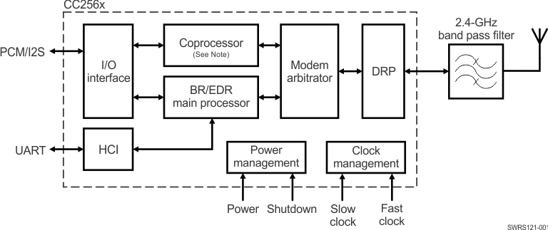
1.4 Functional Block Diagram
