SNVS846G June 2012 – November 2017 LM34925
PRODUCTION DATA.
- 1 Features
- 2 Applications
- 3 Description
- 4 Revision History
- 5 Pin Configuration and Functions
- 6 Specifications
-
7 Detailed Description
- 7.1 Overview
- 7.2 Functional Block Diagram
- 7.3
Feature Description
- 7.3.1 Control Overview
- 7.3.2 VCC Regulator
- 7.3.3 Regulation Comparator
- 7.3.4 Overvoltage Comparator
- 7.3.5 On-Time Generator
- 7.3.6 Current Limit
- 7.3.7 N-Channel Buck Switch and Driver
- 7.3.8 Synchronous Rectifier
- 7.3.9 Undervoltage Detector
- 7.3.10 Thermal Protection
- 7.3.11 Ripple Configuration
- 7.3.12 Soft Start
- 7.4 Device Functional Modes
-
8 Application and Implementation
- 8.1 Application Information
- 8.2
Typical Application
- 8.2.1
Application Circuit: 20-V to 95-V Input and 10-V, 100-mA Output Isolated Fly-Buck Converter
- 8.2.1.1 Design Requirements
- 8.2.1.2
Detailed Design Procedure
- 8.2.1.2.1 Transformer Turns Ratio
- 8.2.1.2.2 Total IOUT
- 8.2.1.2.3 RFB1, RFB2
- 8.2.1.2.4 Frequency Selection
- 8.2.1.2.5 Transformer Selection
- 8.2.1.2.6 Primary Output Capacitor
- 8.2.1.2.7 Secondary Output Capacitor
- 8.2.1.2.8 Type III Feedback Ripple Circuit
- 8.2.1.2.9 Secondary Diode
- 8.2.1.2.10 VCC and Bootstrap Capacitor
- 8.2.1.2.11 Input Capacitor
- 8.2.1.2.12 UVLO Resistors
- 8.2.1.2.13 VCC Diode
- 8.2.2 Application Curves
- 8.2.1
Application Circuit: 20-V to 95-V Input and 10-V, 100-mA Output Isolated Fly-Buck Converter
- 9 Power Supply Recommendations
- 10Layout
- 11Device and Documentation Support
- 12Mechanical, Packaging, and Orderable Information
パッケージ・オプション
メカニカル・データ(パッケージ|ピン)
サーマルパッド・メカニカル・データ
発注情報
1 Features
- Wide 7.5-V to 100-V Input Range
- Integrated 100-mA High-Side,
and Low-Side Switches - No Schottky Required
- Constant On-Time Control
- No Loop Compensation Required
- Ultra-Fast Transient Response
- Nearly Constant Operating Frequency
- Intelligent Peak Current Limit
- Adjustable Output Voltage From 1.225 V
- Precision 2% Feedback Reference
- Frequency Adjustable to 1 MHz
- Adjustable Undervoltage Lockout (UVLO)
- Remote Shutdown
- Thermal Shutdown
- Packages:
- 8-Pin WSON
- 8-Pin SO PowerPAD™
2 Applications
- Isolated Telecom Bias Supply
- Isolated Automotive and Industrial Electronics
3 Description
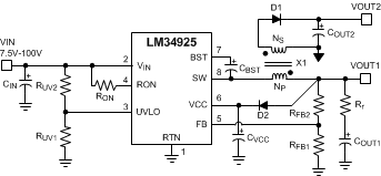
The LM34925 regulator features all of the functions needed to implement a low cost, efficient, isolated bias regulator. This high voltage regulator contains two 100-V N-Channel MOSFET switches: a high-side buck switch and a low-side synchronous switch. The constant-on-time (COT) control scheme employed in the LM34925 device requires no loop compensation and provides excellent transient response. The regulator operates with an on-time that is inversely proportional to the input voltage. This feature allows the operating frequency to remain relatively constant. An intelligent peak current limit is implemented with integrated sense circuit. Other features include a programmable input under voltage comparator to inhibit operation during low-voltage conditions. Protection features include thermal shutdown and VCC undervoltage lockout (UVLO). The LM34925 device is offered in 8-pin WSON and
8-pin SO PowerPAD plastic packages.
Device Information(1)
| PART NUMBER | PACKAGE | BODY SIZE (NOM) |
|---|---|---|
| LM34925 | SO PowerPAD (8) | 4.89 mm × 3.90 mm |
| WSON (8) | 4.00 mm × 4.00 mm |
- For all available packages, see the orderable addendum at the end of the data sheet.
Typical Application Schematic
