SNAS513F August 2011 – November 2015 LM48560
PRODUCTION DATA.
- 1 Features
- 2 Applications
- 3 Description
- 4 Revision History
- 5 Pin Configuration and Functions
- 6 Specifications
- 7 Parameter Measurement Information
- 8 Detailed Description
- 9 Application and Implementation
- 10Power Supply Recommendations
- 11Layout
- 12Device and Documentation Support
- 13Mechanical, Packaging, and Orderable Information
1 Features
- Class H Topology
- Integrated Boost Converter
- Bridge-Tied Load (BTL) Output
- Selectable Differential Inputs
- Selectable Control Interfaces
- (Hardware or Software mode)
- I2C Programmable ALC
- Low Supply Current
- Minimum External Components
- Micro-Power Shutdown
- Available in Space-Saving DSBGA Package
- Key Specifications:
- Output Voltage at VDD = 3.6 V,
RL = 1.5 μF + 10 Ω, THD+N ≤ 1%- 30 VP-P (Typical)
- Quiescent Power Supply Current
at 3.6 V (ALC Enabled)- 4 mA (Typical)
- Power Dissipation at 25 VP-P, 1 W (Typical)
- Shutdown Current, 0.1 μA (Typical)
- Output Voltage at VDD = 3.6 V,
2 Applications
- Touch Screen Smart Phones
- Tablet PCs
- Portable Electronic Devices
- MP3 Players
3 Description
The LM48560 device is a high voltage, high efficiency, Class H driver for ceramic speakers and piezo actuators. The LM48560 device’s Class H architecture offers significant power savings compared to traditional Class AB amplifiers. The device provides 30 VP-P output drive while consuming just 4 mA of quiescent current from a 3.6 V supply.
The LM48560 device features TI’s unique automatic level control (ALC) that provides output limiter functionality. The LM48560 device features two fully differential inputs with separate gain settings, and a selectable control interface. In software control mode, the gain control and device modes are configured through the I2C interface. In hardware control mode, the gain and input mux are configured through a pair of logic inputs.
The LM48560 device has a low power shutdown mode that reduces quiescent current consumption to 0.1 μA. The LM48560 device is available in an ultra-small 16–bump DSBGA package (1.97 mm × 1.97 mm).
Device Information(1)
| PART NUMBER | PACKAGE | BODY SIZE (NOM) |
|---|---|---|
| LM48560 | DSBGA (16) | 1.97 mm × 1.97 mm |
- For all available packages, see the orderable addendum at the end of the data sheet.
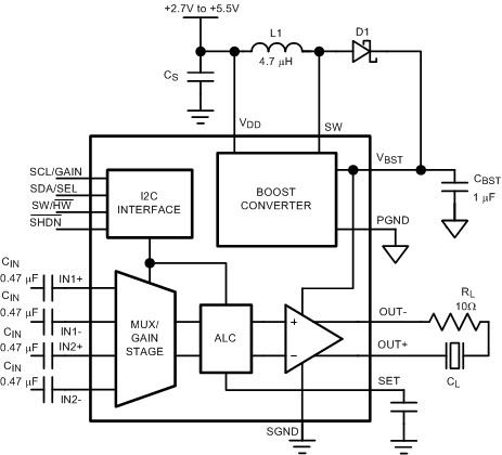
Typical Application Circuit

4 Revision History
| Rev | Date | Description |
|---|---|---|
| 1.0 | 08/16/11 | Initial WEB released. |
| 1.01 | 09/21/11 | Input edits under CLASS H OPERATION. |
| 1.02 | 11/01/11 | Edited curves 30150753, 54, 55, 56, and Figure 26 (I2C Read Cycle). |
| 1.03 | 11/10/11 | Edited Figure 26. |
| 1.04 | 07/25/12 | Input texts/limits edits in the EC table. |
| 1.05 | 08/22/12 | Edited Table 1 and Table 2. |
| E | 05/02/2013 | Changed layout of National Data Sheet to TI format. |
| F | 10/21/2015 | Added ESD Ratings table, Feature Description section, Device Functional Modes, Application and Implementation section, Power Supply Recommendations section, Layout section, Device and Documentation Support section, and Mechanical, Packaging, and Orderable Information section. |