-
LMX2487E 7.5-GHz, High-Performance, Delta-Sigma Low-Power Dual PLLatinum Frequency Synthesizers With 3-GHz Integer PLL
- 1 Features
- 2 Applications
- 3 Description
- 4 Revision History
- 5 Pin Configuration and Functions
- 6 Specifications
- 7 Parameter Measurement Information
-
8 Detailed Description
- 8.1 Overview
- 8.2 Functional Block Diagram
- 8.3 Feature Description
- 8.4 Device Functional Modes
- 8.5 Programming
- 8.6
Register Maps
- 8.6.1 R0 Register
- 8.6.2 R1 REGISTER
- 8.6.3 R2 Register
- 8.6.4 R3 Register
- 8.6.5
R4 Register
- 8.6.5.1 MUX[3:0] Frequency Out and Lock Detect MUX
- 8.6.5.2 IF_P - IF Prescaler
- 8.6.5.3 RF_CPP - RF PLL Charge Pump Polarity
- 8.6.5.4 IF_CPP - IF PLL Charge Pump Polarity
- 8.6.5.5 OSC_OUT Oscillator Output Buffer Enable
- 8.6.5.6 OSC2X - Oscillator Doubler Enable
- 8.6.5.7 FM[1:0] - Fractional Mode
- 8.6.5.8 DITH[1:0] - Dithering Control
- 8.6.5.9 ATPU - PLL Automatic Power Up
- 8.6.6 R5 Register
- 8.6.7 R6 Register
- 8.6.8 R7 Register
- 9 Application and Implementation
- 10Power Supply Recommendations
- 11Layout
- 12Device and Documentation Support
- 13Mechanical, Packaging, and Orderable Information
- IMPORTANT NOTICE
パッケージ・オプション
メカニカル・データ(パッケージ|ピン)
- RTW|24
サーマルパッド・メカニカル・データ
- RTW|24
発注情報
LMX2487E 7.5-GHz, High-Performance, Delta-Sigma Low-Power Dual PLLatinum Frequency Synthesizers With 3-GHz Integer PLL
1 Features
- Quadruple Modulus Prescaler for Lower Divids
- RF PLL: 16/17/20/21 or 32/33/36/37
- IF PLL: 8/9 or 16/17
- Advanced Delta Sigma Fractional Compensation
- 12-Bit or 22-Bit Selectable Fractional Modulus
- Up to 4th Order Programmable Delta-Sigma Modulator
- Features for Improved Lock Time
- Fastlock / Cycle Slip Reduction that Requires Single-Word Write
- Integrated Time-Out Counter
- Wide Operating Range
- LMX2487E RF PLL: 3.0 GHz to 7.5 GHz
- Useful Features
- Digital Lock Detect Output
- Hardware and Software Power-Down Control
- On-Chip Crystal Reference Frequency Doubler
- RF Phase Comparison Frequency Up to 50 MHz
- 2.5-V to 3.6-V Operation With ICC = 8.5 mA at 3.0 V
2 Applications
- Cellular Phones and Base Stations
- Direct Digital Modulation Applications
- Satellite and Cable TV Tuners
- WLAN Standards
3 Description
The LMX2487E device is a low power, high performance delta-sigma fractional-N PLL with an auxiliary integer-N PLL. It is fabricated using TI’s advanced process.
With delta-sigma architecture, fractional spurs at lower offset frequencies are pushed to higher frequencies outside the loop bandwidth. The ability to push close in spur and phase noise energy to higher frequencies is a direct function of the modulator order. Unlike analog compensation, the digital feedback technique used in the LMX2487E is highly resistant to changes in temperature and variations in wafer processing. The LMX2487E delta-sigma modulator is programmable up to fourth order, which allows the designer to select the optimum modulator order to fit the phase noise, spur, and lock time requirements of the system.
Serial data for programming the LMX2487E is transferred through a three-line, high-speed (20-MHz) MICROWIRE interface. The LMX2487E offers fine frequency resolution, low spurs, fast programming speed, and a single-word write to change the frequency. This makes it ideal for direct digital modulation applications, where the N-counter is directly modulated with information. The LMX2487E is available in a 24-lead 4.0 × 4.0 × 0.8 mm WQFN package.
Device Information(1)
| PART NUMBER | PACKAGE | BODY SIZE (NOM) |
|---|---|---|
| LMX2487E | WQFN (24) | 4.00 mm × 4.00 mm |
- For all available packages, see the orderable addendum at the end of the data sheet.
Functional Block Diagram

4 Revision History
Changes from A Revision (March 2013) to B Revision
- Added Pin Configuration and Functions section, ESD Ratings table, Feature Description section, Device Functional Modes, Application and Implementation section, Power Supply Recommendations section, Layout section, Device and Documentation Support section, and Mechanical, Packaging, and Orderable Information section Go
Changes from * Revision (March 2013) to A Revision
- Changed layout of National Data Sheet to TI formatGo
5 Pin Configuration and Functions
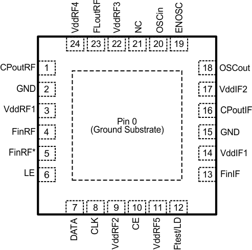
Pin Functions
| PIN | I/O | DESCRIPTION | |
|---|---|---|---|
| NO. | NAME | ||
| 0 | GND | — | Ground Substrate. This is on the bottom of the package and must be grounded. |
| 1 | CPoutRF | O | RF PLL charge pump output. |
| 2 | GND | — | RF PLL analog ground. |
| 3 | VddRF1 | — | RF PLL analog power supply. |
| 4 | FinRF | I | RF PLL high-frequency input pin. |
| 5 | FinRF* | I | RF PLL complementary high-frequency input pin. Shunt to ground with a 100-pF capacitor. |
| 6 | LE | I | MICROWIRE Load Enable. High-impedance CMOS input. Data stored in the shift registers is loaded into the internal latches when LE goes HIGH |
| 7 | DATA | I | MICROWIRE Data. High-impedance binary serial data input. |
| 8 | CLK | I | MICROWIRE Clock. High-impedance CMOS Clock input. Data for the various counters is clocked into the 24-bit shift register on the rising edge |
| 9 | VddRF2 | — | Power supply for RF PLL digital circuitry. |
| 10 | CE | I | Chip Enable control pin. Must be pulled high for normal operation. |
| 11 | VddRF5 | I | Power supply for RF PLL digital circuitry. |
| 12 | Ftest/LD | O | Test frequency output / Lock Detect. |
| 13 | FinIF | I | IF PLL high-frequency input pin. |
| 14 | VddIF1 | — | IF PLL analog power supply. |
| 15 | GND | — | IF PLL digital ground. |
| 16 | CPoutIF | O | IF PLL charge pump output |
| 17 | VddIF2 | — | IF PLL power supply. |
| 18 | OSCout | O | Buffered output of the OSCin signal. |
| 19 | ENOSC | I | Oscillator enable. When this is set to high, the OSCout pin is enabled regardless of the state of other pins or register bits. |
| 20 | OSCin | I | Reference Input. |
| 21 | NC | I | This pin must be left open. |
| 22 | VddRF3 | — | Power supply for RF PLL digital circuitry. |
| 23 | FLoutRF | O | RF PLL Fastlock Output. Also functions as Programmable TRI-STATE CMOS output. |
| 24 | VddRF4 | — | RF PLL analog power supply. |
6 Specifications
6.1 Absolute Maximum Ratings
See (1).| MIN | MAX | UNIT | ||
|---|---|---|---|---|
| VCC | Power supply voltage | –0.3 | 4.25 | V |
| Vi | Voltage on any pin with GND = 0 V | –0.3 | VCC + 0.3 | V |
| TL | Lead temperature (Solder 4 sec.) | 260 | °C | |
| Tstg | Storage temperature | –65 | 150 | °C |
6.2 ESD Ratings
| VALUE | UNIT | |||
|---|---|---|---|---|
| V(ESD) | Electrostatic discharge(1) | Human-body model (HBM) | ±2000 | V |
| Charged-device model (CDM) | ±750 | |||
| Machine model (MM) | ±200 | |||
6.3 Recommended Operating Conditions
| MIN | NOM | MAX | UNIT | ||
|---|---|---|---|---|---|
| VCC | Power supply voltage (1) | 2.5 | 3 | 3.6 | V |
| TA | Operating temperature | -40 | 25 | 85 | °C |
6.4 Thermal Information
| THERMAL METRIC(1) | LMX2485, LMX2485E | UNIT | |
|---|---|---|---|
| RTW (WQFN) | |||
| 24 PINS | |||
| RθJA | Junction-to-ambient thermal resistance | 47.2 | °C/W |
| RθJC(top) | Junction-to-case (top) thermal resistance | 43 | °C/W |
| RθJB | Junction-to-board thermal resistance | 24 | °C/W |
| ψJT | Junction-to-top characterization parameter | 0.8 | °C/W |
| ψJB | Junction-to-board characterization parameter | 24 | °C/W |
| RθJC(bot) | Junction-to-case (bottom) thermal resistance | 7 | °C/W |
6.5 Electrical Characteristics
(VCC = 3.0V; -40°C ≤ TA ≤ +85°C unless otherwise specified)| PARAMETER | TEST CONDITIONS | MIN | TYP | MAX | UNIT | |||
|---|---|---|---|---|---|---|---|---|
| ICC PARAMETERS | ||||||||
| ICCRF | Power supply current, RF synthesizer | IF PLL OFF RF PLL ON Charge pump TRI-STATE |
5.7 | mA | ||||
| ICCIF | Power supply current, IF synthesizer | IF PLL ON RF PLL OFF Charge pump TRI-STATE |
2.5 | mA | ||||
| ICCTOTAL | Power supply current, entire synthesizer | IF PLL ON RF PLL ON Charge pump TRI-STATE |
8.5 | mA | ||||
| ICCPD | Power-down current | CE = ENOSC = 0 V CLK, DATA, LE = 0 V |
< 1 | µA | ||||
| RF SYNTHESIZER PARAMETERS | ||||||||
| fFinRF | Operating frequency | LMX2487E | RF_P = 16 | 3000 | 4000 | MHz | ||
| RF_P = 32 | 3000 | 7500 | ||||||
| pFinRF | Input sensitivity | 3-6 GHz | -10 | 0 | dBm | |||
| 6-7.5 GHz | -5 | 5 | ||||||
| fCOMP | Phase detector frequency(1) | 50 | MHz | |||||
| ICPoutRFSRCE | RF charge pump source current(2) | RF_CPG = 0 VCPoutRF = VCC/2 |
95 | µA | ||||
| RF_CPG = 1 VCPoutRF = VCC/2 |
190 | µA | ||||||
| ... | ... | µA | ||||||
| RF_CPG = 15 VCPoutRF = VCC/2 |
1520 | µA | ||||||
| ICPoutRFSINK | RF charge pump sink current(2) | RF_CPG = 0 VCPoutRF = VCC/2 |
–95 | µA | ||||
| RF_CPG = 1 VCPoutRF = VCC/2 |
–190 | µA | ||||||
| ... | ... | µA | ||||||
| RF_CPG = 15 VCPoutRF = VCC/2 |
–1520 | µA | ||||||
| ICPoutRFTRI | RF charge pump TRI-STATE current magnitude | 0.5 ≤ VCPoutRF ≤ VCC -0.5 | 2 | 10 | nA | |||
| | ICPoutRF%MIS | | Magnitude of RF CP sink vs CP source mismatch | VCPoutRF = VCC/2 TA = 25°C |
RF_CPG > 2 | 3% | 10% | |||
| RF_CPG ≤ 2 | 3% | 13% | ||||||
| | ICPoutRF%V | | Magnitude of RF CP current vs CP voltage | 0.5 ≤ VCPoutRF ≤ VCC -0.5 TA = 25°C |
2% | 8% | ||||
| | ICPoutRF%T | | Magnitude of RF CP current vs temperature | VCPoutRF = VCC/2 | 4% | |||||
| IF SYNTHESIZER PARAMETERS | ||||||||
| fFinIF | Operating frequency | IF_P = 8 | 250 | 2000 | MHz | |||
| IF_P = 16 | 250 | 3000 | ||||||
| pFinIF | IF input sensitivity | –10 | 5 | dBm | ||||
| fCOMP | Phase detector frequency | 10 | MHz | |||||
| ICPoutIFSRCE | IF charge pump source current | VCPoutIF = VCC/2 | 3.5 | mA | ||||
| ICPoutIFSINK | IF charge pump sink current | VCPoutIF = VCC/2 | –3.5 | mA | ||||
| ICPoutIFTRI | IF charge pump TRI-STATE current magnitude | 0.5 ≤ VCPoutIF ≤ VCC RF – 0.5 | 2 | 10 | nA | |||
| | ICPoutIF%MIS | | Magnitude of IF CP sink vs CP source mismatch | VCPoutIF = VCC/2 TA = 25°C |
1% | 8% | ||||
| | ICPoutIF%V | | Magnitude of IF CP current vs CP voltage | 0.5 ≤ VCPoutIF ≤ VCC – 0.5 TA = 25°C |
4% | 10% | ||||
| | ICPoutIF%TEMP | Magnitude of IF CP current vs temperature | VCPoutIF = VCC/2 | 4% | |||||
| OSCILLATOR PARAMETERS | ||||||||
| fOSCin | Oscillator operating frequency | OSC2X = 0 | 5 | 110 | MHz | |||
| OSC2X = 1 | 5 | 20 | MHz | |||||
| vOSCin | Oscillator input sensitivity | 0.5 | VCC | VP-P | ||||
| IOSCin | Oscillator input current | –100 | 100 | µA | ||||
| SPURS | ||||||||
| Spurs in band(3) | -55 | dBc | ||||||
| PHASE NOISE | ||||||||
| LF1HzRF | RF synthesizer normalized phase noise contribution(4) | RF_CPG = 0 | –202 | dBc/Hz | ||||
| RF_CPG = 1 | –204 | |||||||
| RF_CPG = 3 | –206 | |||||||
| RF_CPG = 7 | –210 | |||||||
| RF_CPG = 15 | –210 | |||||||
| LF1HzIF | IF synthesizer normalized phase noise contribution | –209 | dBc/Hz | |||||
| DIGITAL INTERFACE (DATA, CLK, LE, ENOSC, CE, Ftest/LD, FLoutRF) | ||||||||
| VIH | High-level input voltage | 1.6 | VCC | V | ||||
| VIL | Low-level input voltage | 0.4 | V | |||||
| IIH | High-level input current | VIH = VCC | –1 | 1 | µA | |||
| IIL | Low-level input current | VIL = 0 V | –1 | 1 | µA | |||
| VOH | High-level output voltage | IOH = –500 µA | VCC – 0.4 | V | ||||
| VOL | Low-level output voltage | IOL = 500 µA | 0.4 | V | ||||
6.6 Timing Requirements
| MIN | NOM | MAX | UNIT | |||
|---|---|---|---|---|---|---|
| MICROWIRE INTERFACE TIMING | ||||||
| tCS | Data to clock set-up time | See Figure 1 | 25 | ns | ||
| tCH | Data to clock hold time | See Figure 1 | 8 | ns | ||
| tCWH | Clock pulse width high | See Figure 1 | 25 | ns | ||
| tCWL | Clock pulse width low | See Figure 1 | 25 | ns | ||
| tES | Clock to load enable set-up time | See Figure 1 | 25 | ns | ||
| tEW | Load enable pulse width | See Figure 1 | 25 | ns | ||
 Figure 1. MICROWIRE Input Timing Diagram
6.7 Typical Characteristics
6.7.1 Sensitivity
Typical characteristics do not imply any sort of ensured specification. Ensured specifications are in Electrical Characteristics.
| TA = 25°C, RF_P = 32 |

| TA = 25°C, IF_P = 16 |

| TA = 25°C, OSC_2X = 0 |


| VCC = 3 V, RF_P = 32 |

| VCC = 3 V, IF_P = 16 |

| VCC = 3 V, OSC_2X = 0 |

6.7.2 FinRF Input Impedance
Typical characteristics do not imply any sort of ensured specification. Ensured specifications are in Electrical Characteristics. Figure 10. FinRF Input Impedance
Table 1. RF PLL Input Impedance
| FinRF INPUT IMPEDANCE | ||
|---|---|---|
| FREQUENCY (MHz) | REAL (Ω) | IMAGINARY (Ω) |
| 3000 | 39 | –94 |
| 3200 | 37 | –86 |
| 3400 | 33 | –78 |
| 3600 | 30 | –72 |
| 3800 | 28 | –69 |
| 4000 | 26 | –66 |
| 4250 | 24 | –63 |
| 4500 | 23 | –60 |
| 4750 | 22 | –57 |
| 5000 | 20 | –54 |
| 5250 | 19 | –50 |
| 5500 | 18 | –49 |
| 5750 | 17 | –47 |
| 6000 | 17 | –45 |
| 6250 | 16 | –44 |
| 6500 | 16 | –42 |
| 6750 | 16 | –40 |
| 7000 | 16 | –39 |
| 7250 | 16 | –37 |
| 7500 | 16 | –35 |
| 7750 | 17 | –33 |
| 8000 | 17 | –30 |
| 8250 | 16 | –27 |
6.7.3 FinIF Input Impedance
Typical characteristics do not imply any sort of ensured specification. Ensured specifications are in Electrical Characteristics. Figure 11. FinIF Input Impedance
Table 2. IF PLL Input Impedance
| FinIF INPUT IMPEDANCE | ||
|---|---|---|
| FREQUENCY (MHz) | REAL (Ω) | IMAGINARY (Ω) |
| 100 | 508 | –233 |
| 150 | 456 | –215 |
| 200 | 420 | –206 |
| 250 | 403 | –205 |
| 300 | 370 | –207 |
| 400 | 344 | –215 |
| 500 | 207 | –223 |
| 600 | 274 | –225 |
| 700 | 242 | –225 |
| 800 | 242 | –225 |
| 900 | 214 | –222 |
| 1000 | 171 | –208 |
| 1200 | 137 | –191 |
| 1400 | 112 | –176 |
| 1600 | 91 | –158 |
| 1800 | 76 | –139 |
| 2000 | 62 | –122 |
| 2200 | 51 | –105 |
| 2300 | 46 | –96 |
| 2400 | 42 | –88 |
| 2600 | 37 | –74 |
| 2800 | 29 | –63 |
| 3000 | 25 | –54 |
6.7.4 OSCin Input Impedance
Typical characteristics do not imply any sort of ensured specification. Ensured specifications are in Electrical Characteristics. Figure 12. OSCin Input Impedance
Table 3. OSCin Input Impedance
| FREQUENCY (MHz) | POWERED UP | POWERED DOWN | ||||
|---|---|---|---|---|---|---|
| REAL | IMAGINARY | MAGNITUDE | REAL | IMAGINARY | MAGNITUDE | |
| 5 | 1730 | –3779 | 4157 | 392 | –8137 | 8146 |
| 10 | 846 | –2236 | 2391 | 155 | –4487 | 4490 |
| 20 | 466 | –1196 | 1284 | 107 | –2215 | 2217 |
| 30 | 351 | –863 | 932 | 166 | –1495 | –1504 |
| 40 | 316 | –672 | 742 | 182 | –1144 | 1158 |
| 50 | 278 | –566 | 631 | 155 | –912 | 925 |
| 60 | 261 | –481 | 547 | 153 | –758 | 774 |
| 70 | 252 | –425 | 494 | 154 | –652 | 669 |
| 80 | 239 | –388 | 456 | 147 | –576 | 595 |
| 90 | 234 | –358 | 428 | 145 | –518 | 538 |
| 100 | 230 | –337 | 407 | 140 | –471 | 492 |
| 110 | 225 | –321 | 392 | 138 | –436 | 458 |
| 120 | 219 | –309 | 379 | 133 | –402 | 123 |
| 130 | 214 | –295 | 364 | 133 | –374 | 397 |
| 140 | 208 | –285 | 353 | 132 | –349 | 373 |
| 150 | 207 | –279 | 348 | 133 | –329 | 355 |
6.7.5 Currents
Typical characteristics do not imply any sort of ensured specification. Ensured specifications are in Electrical Characteristics.
| CE = High |


| VCC = 3 V |


| VCC = 3 V |
7 Parameter Measurement Information
7.1 Bench Test Set-Ups
7.1.1 Charge Pump Current Measurement
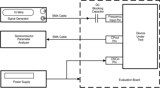 Figure 18. Charge Pump Current Measurement
Figure 18 shows the test procedure for testing the RF and IF charge pumps. These tests include absolute current level, mismatch, and leakage measurement. In order to measure the charge pump currents, a signal is applied to the high frequency input pins. The reason for this is to ensure that the phase detector gets enough transitions in order to be able to change states. If no signal is applied, it is possible that the charge pump current reading will be low due to the fact that the duty cycle is not 100%. The OSCin Pin is tied to the supply. The charge pump currents can be measured by simply programming the phase detector to the necessary polarity. For instance, in order to measure the RF charge pump, a 10-MHz signal is applied to the FinRF pin. The source current can be measured by setting the RF PLL phase detector to a positive polarity, and the sink current can be measured by setting the phase detector to a negative polarity. The IF PLL currents can be measured in a similar way.
NOTE
The magnitude of the RF PLL charge pump current is controlled by the RF_CPG bit. Once the charge pump currents are known, the mismatch can be calculated as well. In order to measure leakage, the charge pump is set to a TRI-STATE mode by enabling the RF_CPT and IF_CPT bits. The table below shows a summary of the various charge pump tests.
Table 4. Charge Pump Test Programming
| CURRENT TEST | RF_CPG | RF_CPP | RF_CPT | IF_CPP | IF_CPT |
|---|---|---|---|---|---|
| RF Source | 0 to 15 | 0 | 0 | X | X |
| RF Sink | 0 to 15 | 1 | 0 | X | X |
| RF TRI-STATE | X | X | 1 | X | X |
| IF Source | X | X | X | 0 | 0 |
| IF Sink | X | X | X | 1 | 0 |
| IF TRI-STATE | X | X | X | X | 1 |
7.1.2 Charge Pump Current Specification Definitions
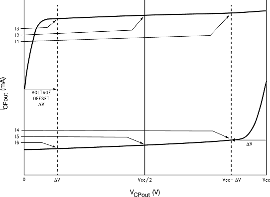 Figure 19. Charge Pump Definitions
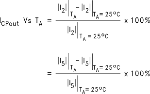
I1 = Charge Pump Sink Current at VCPout = Vcc – ΔV
I2 = Charge Pump Sink Current at VCPout = Vcc/2
I3 = Charge Pump Sink Current at VCPout = ΔV
I4 = Charge Pump Source Current at VCPout = Vcc – ΔV
I5 = Charge Pump Source Current at VCPout = Vcc/2
I6 = Charge Pump Source Current at VCPout = ΔV
ΔV = Voltage offset from the positive and negative supply rails. Defined to be 0.5 V for this part.
vCPout refers to either VCPoutRF or VCPoutIF
ICPout refers to either ICPoutRF or ICPoutIF
7.1.2.1 Charge Pump Output Current Variation vs Charge Pump Output Voltage
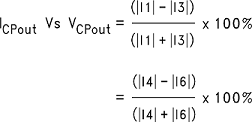
Charge Pump Sink Current vs Charge Pump Output Source Current Mismatch

7.1.2.2 Charge Pump Output Current Variation vs Temperature
7.1.3 Sensitivity Measurement
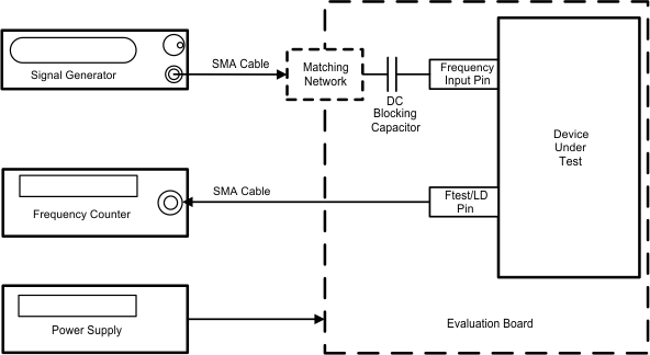 Figure 20. Setup for Sensitivity Measurement
Table 5. Settings for Sensitivity Measurement
| FREQUENCY INPUT PIN | DC-BLOCKING CAPACITOR | CORRESPONDING COUNTER | DEFAULT COUNTER VALUE | MUX VALUE |
|---|---|---|---|---|
| OSCin | 1000 pF | RF_R / 2 | 50 | 14 |
| FinRF | 100 pF// 1000 pF | RF_N / 2 | 502 + 2097150 / 4194301 | 15 |
| FinIF | 100 pF | IF_N / 2 | 534 | 13 |
| OSCin | 1000 pF | IF_R / 2 | 50 | 12 |
Sensitivity is defined as the power level limits beyond which the output of the counter being tested is off by 1 Hz or more of its expected value. It is typically measured over frequency, voltage, and temperature. In order to test sensitivity, the MUX[3:0] word is programmed to the appropriate value. The counter value is then programmed to a fixed value and a frequency counter is set to monitor the frequency of this pin. The expected frequency at the Ftest/LD pin should be the signal generator frequency divided by twice the corresponding counter value. The factor of two comes in because the LMX2487E has a flip-flop which divides this frequency by two to make the duty cycle 50% in order to make it easier to read with the frequency counter. The frequency counter input impedance should be set to high impedance. In order to perform the measurement, the temperature, frequency, and voltage is set to a fixed value and the power level of the signal is varied.
NOTE
The power level at the part is assumed to be 4 dB less than the signal generator power level. This accounts for 1 dB for cable losses and 3 dB for the pad.
The power level range where the frequency is correct at the Ftest/LD pin to within 1 Hz accuracy is recorded for the sensitivity limits. The temperature, frequency, and voltage can be varied in order to produce a family of sensitivity curves. Because this is an open-loop test, the charge pump is set to TRI-STATE and the unused side of the PLL (RF or IF) is powered down when not being tested. For this part, there are actually four frequency input pins, although there is only one frequency test pin (Ftest/LD). The conditions specific to each pin are shown in the table in the Charge Pump Current Specification Definitions section.
NOTE
That for the RF N counter, a fourth order fractional modulator is used in 22-bit mode with a fraction of 2097150 / 4194301 is used. The reason for this long fraction is to test the RF N counter and supporting fractional circuitry as completely as possible.
7.1.4 Input Impedance Measurement
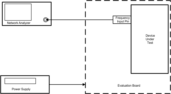 Figure 21. Input Impedance Measurement
Figure 21 shows the test set-up used for measuring the input impedance for the LMX2487E. The DC-blocking capacitor used between the input SMA connector and the pin being measured must be changed to a 0-Ω resistor. This procedure applies to the FinRF, FinIF, and OSCin pins. The basic test procedure is to calibrate the network analyzer, ensure that the part is powered up, and then measure the input impedance. The network analyzer can be calibrated by using either calibration standards or by soldering resistors directly to the evaluation board. An open can be implemented by putting no resistor, a short can be implemented by soldering a 0-Ω resistor as close as possible to the pin being measured, and a short can be implemented by soldering two 100-Ω resistors in parallel as close as possible to the pin being measured. Calibration is done with the PLL removed from the PCB. This requires the use of a clamp down fixture that may not always be generally available. If no clamp down fixture is available, then this procedure can be done by calibrating up to the point where the DC-blocking capacitor usually is, and then implementing port extensions with the network analyzer. The 0-Ω resistor is added back for the actual measurement. Once the set-up is calibrated, it is necessary to ensure that the PLL is powered up. This can be done by toggling the power down bits (RF_PD and IF_PD) and observing that the current consumption indeed increases when the bit is disabled. Sometimes it may be necessary to apply a signal to the OSCin pin in order to program the part. If this is necessary, disconnect the signal once it is established that the part is powered up. It is useful to know the input impedance of the PLL for the purposes of debugging RF problems and designing matching networks. Another use of knowing this parameter is make the trace width on the PCB such that the input impedance of this trace matches the real part of the input impedance of the PLL frequency of operation. In general, it is good practice to keep trace lengths short and make designs that are relatively resistant to variations in the input impedance of the PLL.