SNVSA15B December   2013  – December 2015 LP8557

PRODUCTION DATA.  

  1. Features
  2. Applications
  3. Description
  4. Revision History
  5. Device Comparison Table
  6. Pin Function and Configurations
  7. Specifications
    1. 7.1  Absolute Maximum Ratings
    2. 7.2  ESD Ratings
    3. 7.3  Recommended Operating Conditions
    4. 7.4  Thermal Information
    5. 7.5  Electrical Characteristics
    6. 7.6  Boost Converter Electrical Characteristics
    7. 7.7  LED Driver Electrical Characteristics (LED1 To LED6 Pins)
    8. 7.8  PWM Interface Characteristics (PWM Pin)
    9. 7.9  Logic Interface Characteristics (PWM, FSET/SDA, ISET/SCL Pins)
    10. 7.10 I2C Serial Bus Timing Parameters (SDA, SCL)
    11. 7.11 Typical Characteristics
  8. Detailed Description
    1. 8.1 Overview
    2. 8.2 Functional Block Diagram
    3. 8.3 Feature Description
      1. 8.3.1 Boost Converter Overview
        1. 8.3.1.1 Operation
        2. 8.3.1.2 Adaptive Boost Output Voltage Control
      2. 8.3.2 Brightness Control
        1. 8.3.2.1 PWM Input Duty Measurement
        2. 8.3.2.2 BRTMODE = 00b
        3. 8.3.2.3 BRTMODE = 01b
        4. 8.3.2.4 BRTMODE = 10b
        5. 8.3.2.5 BRTMODE = 11b
        6. 8.3.2.6 Hybrid PWM & I Dimming Control
        7. 8.3.2.7 Phase Shift PWM Scheme
      3. 8.3.3 Slope and Advanced Slope
      4. 8.3.4 LED String Count Auto Detection
      5. 8.3.5 EMI Reduction Schemes
      6. 8.3.6 Fault Detection
        1. 8.3.6.1 LED Short Detection
        2. 8.3.6.2 LED OPEN* Detection
        3. 8.3.6.3 Undervoltage Detection
        4. 8.3.6.4 Thermal Shutdown
        5. 8.3.6.5 Boost Overcurrent Protection
        6. 8.3.6.6 Boost Overvoltage Protection
        7. 8.3.6.7 Boost Undervoltage Protection
    4. 8.4 Device Functional Modes
      1. 8.4.1 Shutdown Mode
      2. 8.4.2 Active Mode
    5. 8.5 Programming
      1. 8.5.1 I2C-Compatible Serial Bus Interface
        1. 8.5.1.1 Interface Bus Overview
        2. 8.5.1.2 Start and Stop Conditions
        3. 8.5.1.3 Data Transactions
        4. 8.5.1.4 Acknowledge Cycle
        5. 8.5.1.5 Acknowledge After Every Byte Rule
        6. 8.5.1.6 Control Register Write Cycle
        7. 8.5.1.7 Control Register Read Cycle
        8. 8.5.1.8 Register Read and Write Detail
    6. 8.6 Register Maps
      1. 8.6.1 Register Bit Descriptions
        1. 8.6.1.1  COMMAND
        2. 8.6.1.2  STATUS
        3. 8.6.1.3  BRTLO
        4. 8.6.1.4  BRTHI
        5. 8.6.1.5  CONFIG
        6. 8.6.1.6  CURRENT
        7. 8.6.1.7  PGEN
        8. 8.6.1.8  BOOST
        9. 8.6.1.9  LEDEN
        10. 8.6.1.10 STEP
  9. Application and Implementation
    1. 9.1 Application Information
      1. 9.1.1 Designing With LP8557
        1. 9.1.1.1 Setting Boost Switching and PWM Dimming Frequencies
        2. 9.1.1.2 Setting Boost Compensation
        3. 9.1.1.3 Setting Full-Scale Led Current
      2. 9.1.2 Designing With LP8557I
        1. 9.1.2.1 Setting Boost Switching Frequency
        2. 9.1.2.2 Setting Boost Compensation
        3. 9.1.2.3 Setting PWM Dimming Frequency
        4. 9.1.2.4 Setting Full-Scale LED Current
    2. 9.2 Typical Applications
      1. 9.2.1 LP8557 PWM-Only Option
        1. 9.2.1.1 Design Requirements
        2. 9.2.1.2 Detailed Design Procedure
          1. 9.2.1.2.1 Boost Output Capacitor Selection
          2. 9.2.1.2.2 Schottky Diode Selection
          3. 9.2.1.2.3 Inductor Selection
          4. 9.2.1.2.4 Boost Input andVDD Capacitor Selection
        3. 9.2.1.3 Application Curves
      2. 9.2.2 LP8557I PWM and I2C Device Option
        1. 9.2.2.1 Design Requirements
        2. 9.2.2.2 Detailed Design Procedure
        3. 9.2.2.3 Application Curves
  10. 10Power Supply Recommendations
  11. 11Layout
    1. 11.1 Layout Guidelines
      1. 11.1.1 Boost Output Capacitor Placement
      2. 11.1.2 Schottky Diode Placement
      3. 11.1.3 Inductor Placement
      4. 11.1.4 Boost Input and VDD Capacitor Placement
    2. 11.2 Layout Example
  12. 12Device and Documentation Support
    1. 12.1 Device Support
      1. 12.1.1 Third-Party Products Disclaimer
    2. 12.2 Related Links
    3. 12.3 Community Resources
    4. 12.4 Trademarks
    5. 12.5 Electrostatic Discharge Caution
    6. 12.6 Glossary
  13. 13Mechanical, Packaging, and Orderable Information

パッケージ・オプション

メカニカル・データ(パッケージ|ピン)
サーマルパッド・メカニカル・データ
発注情報

1 Features

  • High-Efficiency DC-DC Boost Converter With 28-V Integrated Power MOSFET
  • 2.7-V to 5.5-V VDD Range for Supporting Single-Cell Li-Ion Battery Applications
  • Six 25-mA High-Precision LED Current Sinks
  • Adaptive Boost Voltage and LED Current Sink Headroom Controls for Maximum System Efficiency
  • LED String Count Auto-Detect for Maximum Design Flexibility
  • Smart Phase Shift PWM Mode for Reduced Audible Noise
  • PWM Input Duty Cycle Brightness Control, PWM Output Frequency Selectable Independent of Input Frequency
  • Hybrid PWM Plus Current Dimming for Higher LED Drive Optical Efficiency
  • Switching Frequency, PWM Output Frequency, and LED Current can be set Through Resistors or I2C Interface
  • Programmable Boost SW Slew Rate Control and Spread Spectrum Scheme for Reduced Switching Noise and Improved EMI Performance
  • UVLO, TSD, BST_OVP, BST_OCP, BST_UV, LED OPEN* and LED Short Fault Coverage
  • Minimum Number of External Components

2 Applications

    Tablet LCD Display LED Backlight

3 Description

The LP8557 and LP8557I are high-efficiency LED drivers each featuring an integrated DC-DC inductive boost converter and six high-precision current sinks. LP8557 is intended for applications that exclusively use a pulse width modulated (PWM) signal for controlling the brightness while LP8557I is intended for applications that can utilize an I2C master as well.

The boost converter has adaptive output voltage control. This feature minimizes the power consumption by adjusting the voltage to the lowest sufficient level under all conditions.

The adaptive current sink headroom voltage control scales the headroom voltage with the LED current for optimal system efficiency.

The LED string auto-detect function enables use of the same device in systems with 1 to 6 LED strings for the maximum design flexibility.

Proprietary hybrid PWM plus current mode dimming enables additional system power savings. Phase-shift PWM allows reduced audible noise and smaller boost output capacitors.

Flexible CABC support combines brightness level selections based on the PWM input and I2C commands.

Device Information(1)

PART NUMBER PACKAGE BODY SIZE (MAX)
LP8557 DSBGA (16) 1.906 mm x 1.64 mm
LP8557I
  1. For all available packages, see the orderable addendum at the end of the data sheet.

Simplified Schematic With PWM-Only Option
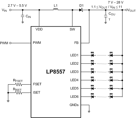
LP8557 LP85571 examplecircuit.gif

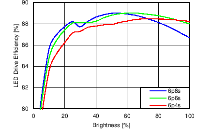
LED Efficiency With 6 LED Strings

LP8557 LP85571 C001_snvs976.png