SNVS542E May 2008 – June 2016 LP8900
PRODUCTION DATA.
- 1 Features
- 2 Applications
- 3 Description
- 4 Revision History
- 5 Default Device Options
- 6 Pin Configuration and Functions
- 7 Specifications
- 8 Detailed Description
- 9 Application and Implementation
- 10Power Supply Recommendations
- 11Layout
- 12Device and Documentation Support
- 13Mechanical, Packaging, and Orderable Information
1 Features
- Input Voltage Operation: 1.8 V to 5.5 V
- Output Voltage: 1.2 V to 3.6 V
- Accuracy Over Temperature: 1%
- Output Voltage Noise: 6 µVRMS
- PSRR: 75 dB at 1 kHz
- Dropout: 110 mV at 200 mA Load
- Quiescent Current: 48 µA per Regulator
- Start-Up Time: 80 µs
- Stable With Ceramic Capacitors as Small as 0402
- Thermal-Overload and Short-Circuit Protection
2 Applications
- Battery-Operated Devices
- Hand-Held Information Appliances
- Noise Sensitive RF Applications
- DC-DC Convertor Post Regulation and Filter
3 Description
The LP8900 is a dual LDO capable of supplying 200-mA output current per regulator. Designed to meet the requirements of RF and analog circuits, the LP8900 provides low device noise, high PSRR, low quiescent current, and superior line transient response figures.
Using new innovative design techniques, the LP8900 offers class-leading device noise performance without a noise bypass capacitor.
The LP8900 is designed to be stable with space saving ceramic capacitors as small as 0402 case size, enabling a solution size < 4 mm2. Performance is specified for a –40°C to +125°C junction temperature range.
Output voltage options from 1.2 V to 3.6 V are available; for availability, contact your local TI sales office.
Device Information(1)
| PART NUMBER | PACKAGE | BODY SIZE (MAX) |
|---|---|---|
| LP8900 | DSBGA (6) | 1.49 mm × 1.09 mm |
- For all available packages, see the orderable addendum at the end of the data sheet.
space
space
space
space
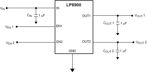
Typical Application Circuit
