SLLS408H January 2000 – October 2016 MAX3222
PRODUCTION DATA.
- 1 Features
- 2 Applications
- 3 Description
- 4 Revision History
- 5 Pin Configuration and Functions
-
6 Specifications
- 6.1 Absolute Maximum Ratings
- 6.2 ESD Ratings
- 6.3 Recommended Operating Conditions
- 6.4 Thermal Information
- 6.5 Electrical Characteristics: Device
- 6.6 Electrical Characteristics: Driver
- 6.7 Electrical Characteristics: Receiver
- 6.8 Switching Characteristics: Driver
- 6.9 Switching Characteristics: Receiver
- 6.10 Typical Characteristics
- 7 Parameter Measurement Information
- 8 Detailed Description
- 9 Application and Implementation
- 10Power Supply Recommendations
- 11Layout
- 12Device and Documentation Support
- 13Mechanical, Packaging, and Orderable Information
パッケージ・オプション
デバイスごとのパッケージ図は、PDF版データシートをご参照ください。
メカニカル・データ(パッケージ|ピン)
- DB|20
- PW|20
- DW|20
サーマルパッド・メカニカル・データ
発注情報
1 Features
- RS-232 Bus-Pin ESD Protection Exceeds ±15 kV Using Human-Body Model (HBM)
- Meets or Exceeds the Requirements of
TIA/EIA-232-F and ITU v.28 Standards - Operates With 3-V to 5.5-V VCC Supply
- Operates Up to 250 kbps
- Two Drivers and Two Receivers
- Low Standby Current: 1 µA Typical
- External Capacitors: 4 × 0.1 µF
- Accepts 5-V Logic Input With 3.3-V Supply
- Alternative High-Speed Pin-Compatible Device
(1 Mbps)- SNx5C3222
2 Applications
- Battery-Powered Systems
- PDAs
- Notebooks
- Laptops
- Palmtop PCs
- Hand-held Equipment
3 Description
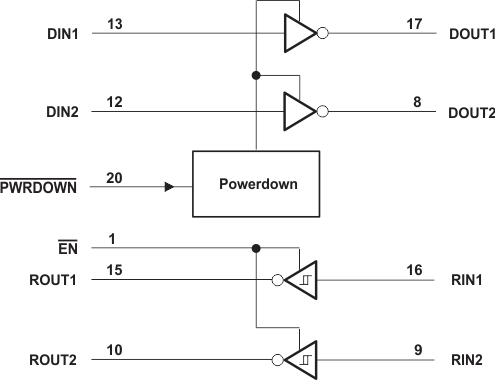
The MAX3222 consists of two line drivers, two line receivers, and a dual charge-pump circuit with ±15-kV ESD protection pin to pin (serial-port connection pins, including GND). The device meets the requirements of TIA/EIA-232-F and provides the electrical interface between an asynchronous communication controller and the serial-port connector. The charge pump and four small external capacitors allow operation from a single 3-V to 5.5-V supply. The device operates at data signaling rates up to 250 kbit/s and a maximum of 30-V/μs driver output slew rate.
The MAX3222 can be placed in the power-down mode by setting PWRDOWN low, which draws only 1 μA from the power supply. When the device is powered down, the receivers remain active while the drivers are placed in the high-impedance state. Receiver outputs also can be placed in the high-impedance state by setting EN high.
Device Information(1)
| PART NUMBER | PACKAGE | BODY SIZE (NOM) |
|---|---|---|
| MAX3222CDW, MAX322IDW | SOIC (20) | 12.80 mm × 7.50 mm |
| MAX3222CDB, MAX322IDB | SSOP (20) | 7.20 mm × 5.30 mm |
| MAX3222CPW, MAX322IPW | TSSOP (20) | 6.50 mm × 4.40 mm |
- For all available packages, see the orderable addendum at the end of the data sheet.
Block Diagram
