SBOS465C January 2009 – January 2016 OPA2348-Q1 , OPA348-Q1 , OPA4348-Q1
PRODUCTION DATA.
The OPAx348-Q1 series of devices are single-supply, low-power CMOS operational amplifiers. Featuring an extended bandwidth of 1 MHz and a supply current of 45 µA, the OPAx348-Q1 family of devices is useful for low-power applications on single supplies of 2.1 V to 5.5 V.
Low supply current of 45 µA and an input bias current of 0.5 pA make the OPAx348-Q1 family of devices an optimal candidate for low-power, high-impedance applications such as smoke detectors and other sensors.
The OPA348-Q1 device is available in both the SOT23-5 (DBV) and the SOIC (D) packages. The OPA2348-Q1 device is available in the SOIC-8 (D) package. The OPA4348-Q1 device is available in the TSSOP-14 (PW) package. The automotive temperature range of –40°C to +125°C over all supply voltages offers additional design flexibility.
PART NUMBER | PACKAGE | BODY SIZE (NOM) |
---|---|---|
OPA348-Q1 | SOT-23 (5) | 2.90 mm × 1.60 mm |
SOIC (8) | 4.90 mm × 3.91 mm | |
OPA2348-Q1 | SOIC (8) | 4.90 mm × 3.91 mm |
OPA4348-Q1 | TSSOP (14) | 5.00 mm × 4.40 mm |
Changes from B Revision (December 2014) to C Revision
Changes from A Revision (January 2009) to B Revision
PIN | I/O | DESCRIPTION | ||
---|---|---|---|---|
NAME | NO. | |||
SOT-23 | SOIC | |||
+IN | 3 | 3 | I | Noninverting input |
–IN | 4 | 2 | I | Inverting input |
OUT | 1 | 6 | O | Output |
V+ | 5 | 7 | — | Positive (highest) supply |
V– | 2 | 4 | — | Negative (lowest) supply |
NC | — | 1 | — | Do not connect |
5 | ||||
8 |
PIN | I/O | DESCRIPTION | |
---|---|---|---|
NAME | NO | ||
+IN A | 3 | I | Noninverting input, Channel A |
–IN A | 2 | I | Inverting input, Channel A |
+IN B | 5 | I | Noninverting input, Channel B |
–IN B | 6 | I | Inverting input, Channel B |
OUT A | 1 | O | Output, Channel A |
OUT B | 7 | O | Output, Channel B |
V+ | 8 | — | Positive (highest) supply |
V– | 4 | — | Negative (lowest) supply |
PIN | I/O | DESCRIPTION | |
---|---|---|---|
NAME | NO. | ||
+IN A | 3 | I | Noninverting input, Channel A |
–IN A | 2 | I | Inverting input, Channel A |
+IN B | 5 | I | Noninverting input, Channel B |
–IN B | 6 | I | Inverting input, Channel B |
+IN C | 10 | I | Noninverting input, Channel C |
–IN C | 9 | I | Inverting input, Channel C |
+IN D | 12 | I | Noninverting input, Channel D |
–IN D | 13 | I | Inverting input, Channel D |
OUT A | 1 | O | Output, Channel A |
OUT B | 7 | O | Output, Channel B |
OUT C | 8 | O | Output, Channel C |
OUT D | 14 | O | Output, Channel D |
V+ | 4 | — | Positive (highest) supply |
V– | 11 | — | Negative (lowest) supply |
MIN | MAX | UNIT | |||
---|---|---|---|---|---|
Supply voltage, VS | V– to V+ | 7.5 | V | ||
Input voltage, VIN | Signal input terminals(2) | (V–) – 0.5 V | (V+) + 0.5 V | V | |
Input current, IIN | Signal input terminals(2) | 10 | mA | ||
Output short-circuit duration(3) | Continuous | ||||
Operating free-air temperature, TA | –40 | 150 | °C | ||
Operating virtual-junction temperature, TJ | 150 | °C | |||
Storage temperature, Tstg | –65 | 150 | °C |
VALUE | UNIT | ||||
---|---|---|---|---|---|
V(ESD) | Electrostatic discharge | Human-body model (HBM), per AEC Q100-002(1) | ±2000 | V | |
Charged-device model (CDM), per AEC Q100-011 | All pins | ±500 | |||
Corner pins (1, 7, 8, and 14) | ±750 |
MIN | MAX | UNIT | ||
---|---|---|---|---|
VS | Supply voltage, V– to V+ | 2.1 | 5.5 | V |
TA | Operating free-air temperature | –40 | 125 | °C |
THERMAL METRIC(1) | OPA348-Q1 | UNIT | ||
---|---|---|---|---|
DBV (SOT-23) | D (SOIC) | |||
5 PINS | 8 PINS | |||
RθJA | Junction-to-ambient thermal resistance | 228.5 | 142.0 | °C/W |
RθJC(top) | Junction-to-case (top) thermal resistance | 99.1 | 90.2 | °C/W |
RθJB | Junction-to-board thermal resistance | 54.6 | 82.5 | °C/W |
ψJT | Junction-to-top characterization parameter | 7.7 | 39.4 | °C/W |
ψJB | Junction-to-board characterization parameter | 53.8 | 82.0 | °C/W |
RθJC(bottom) | Junction-to-case (bottom) thermal resistance | n/a | n/a | °C/W |
THERMAL METRIC(1) | OPA2348-Q1 | OPA4348-Q1 | UNIT | |
---|---|---|---|---|
D (SOIC) | PW (TSSOP) | |||
8 PINS | 14 PINS | |||
RθJA | Junction-to-ambient thermal resistance | 138.4 | 121 | °C/W |
RθJC(top) | Junction-to-case (top) thermal resistance | 89.5 | 49.4 | °C/W |
RθJB | Junction-to-board thermal resistance | 78.6 | 62.8 | °C/W |
ψJT | Junction-to-top characterization parameter | 29.9 | 5.9 | °C/W |
ψJB | Junction-to-board characterization parameter | 78.1 | 62.2 | °C/W |
RθJC(bottom) | Junction-to-case (bottom) thermal resistance | n/a | n/a | °C/W |
PARAMETER | TEST CONDITIONS | TA (1) | MIN | TYP | MAX | UNIT | ||
---|---|---|---|---|---|---|---|---|
VOS | Input offset voltage | VS = 5 V, VCM = (V–) + 0.8 V | 25°C | 1 | 5 | mV | ||
Full range | 6 | |||||||
ΔVOS/ΔT | Offset voltage drift over temperature | Full range | 4 | µV/°C | ||||
PSRR | Offset voltage drift vs power supply | VS = 2.5 V to 5.5 V, VCM < (V+) – 1.7 V | 25°C | 60 | 175 | µV/V | ||
Full range | 300 | |||||||
Channel separation | dc | 25°C | 0.2 | µV/V | ||||
f = 1 kHz | 25°C | 134 | dB | |||||
VCM | Input common-mode voltage range | 25°C | (V–) – 0.2 | (V+) + 0.2 | V | |||
CMRR | Input common-mode rejection ratio | (V–) – 0.2 V < VCM < (V+) – 1.7 V | 25°C | 70 | 82 | dB | ||
Full range | 66 | |||||||
VS = 5.5 V, (V–) – 0.2 V < VCM < (V+) + 0.2 V | 25°C | 60 | 71 | |||||
VS = 5.5 V, (V–) < VCM < (V+) | Full range | 56 | ||||||
IB | Input bias current | 25°C | ±0.5 | ±10 | pA | |||
IOS | Input offset current | 25°C | ±0.5 | ±10 | pA | |||
ZI | Input impedance | Differential | 25°C | 1013|| 3 | Ω || pF | |||
Common-mode | 1013|| 3 | |||||||
Input voltage noise | VCM < (V+) – 1.7 V, f = 0.1 Hz to 10 Hz | 25°C | 10 | µVPP | ||||
Vn | Input voltage noise density | VCM < (V+) – 1.7 V, f = 1 kHz | 25°C | 35 | nV/√Hz | |||
In | Input current noise density | VCM < (V+) – 1.7 V, f = 1 kHz | 25°C | 4 | fA/√Hz | |||
AOL | Open-loop voltage gain | VS = 5 V, RL = 100 kΩ, 0.025 V < VO < 4.975 V |
25°C | 94 | 108 | dB | ||
Full range | 90 | |||||||
VS = 5V, RL = 5 kΩ, 0.125 V < VO < 4.875 V |
25°C | 90 | 98 | |||||
Full range | 88 | |||||||
Voltage output swing from rail | RL = 100 kΩ, AOL > 94 dB | 25°C | 18 | 25 | mV | |||
Full range | 25 | |||||||
RL = 5 kΩ, AOL > 90 dB | 25°C | 100 | 125 | mV | ||||
Full range | 125 | |||||||
ISC | Output short-circuit current | 25°C | ±10 | mA | ||||
CLOAD | Capacitive load drive | See the Typical Characteristics section | 25°C | |||||
GBW | Gain-bandwidth product | CL = 100 pF | 25°C | 1 | MHz | |||
SR | Slew rate | CL = 100 pF, G = +1 | 25°C | 0.5 | V/µs | |||
ts | Settling time | 0.1% | CL = 100 pF, VS = 5.5 V, 2V- step, G = +1 | 25°C | 5 | µs | ||
0.01% | 7 | |||||||
Overload recovery time | VIN × Gain > VS | 25°C | 1.6 | µs | ||||
THD+N | Total harmonic distortion plus noise | CL = 100 pF, VS = 5.5 V, VO = 3 VPP, G = +1, f = 1 kHz |
25°C | 0.0023% | ||||
IQ | Quiescent current | Per amplifier | 25°C | 45 | 65 | µA | ||
Full range | 75 |
Typical production distribution of packaged units. |
G = 1 V/V | RL = 100 kΩ | CL = 100 pF |
VS = ±2.5V |
Typical production distribution of packaged units. |
G = ±5 V/V, RFB = 100 kΩ |
G = 1 V/V | RL = 100 kΩ | CL = 100 pF |
The OPAx348-Q1 family of devices is a low-power, rail-to-rail input and output operational amplifier. These devices operate from 1.8 V to 5.5 V, are unity-gain stable, and are suitable for a wide range of general-purpose applications. The class AB output stage is capable of driving ≤ 10-kΩ loads connected to any point between V+ and ground. The input common-mode voltage range includes both rails and allows the OPAx348-Q1 family of devices to be used in virtually any single-supply application. Rail-to-rail input and output swing significantly increases dynamic range, especially in low-supply applications, and makes them ideal for driving sampling analog-to-digital converters (ADCs).
The OPAx348-Q1 op amp is fully specified and ensured for operation from 1.8 V to 5.5 V. In addition, many specifications apply from –40°C to +125°C. Parameters that vary significantly with operating voltages or temperature are shown in the Typical Characteristics graphs. Power-supply pins should be bypassed with
0.01-μF ceramic capacitors.
The input common-mode voltage range of the OPAx348-Q1 family of devices extends 200 mV beyond the supply rails. This performance is achieved with a complementary input stage: an N-channel input differential pair in parallel with a P-channel differential pair. The N-channel pair is active for input voltages close to the positive rail, typically (V+) – 1.3 V to 200 mV above the positive supply. The P-channel pair is on for inputs from 200 mV below the negative supply to approximately (V+) – 1.3 V. A small transition region exists, typically (V+) – 1.4 V to (V+) – 1.2 V, in which both pairs are on. This 200-mV transition region can vary up to 300 mV with process variation. Thus, the transition region (both stages on) can range from (V+) – 1.7 V to (V+) – 1.5 V on the low end, up to (V+) – 1.1 V to (V+) – 0.9 V on the high end. Within this transition region, PSRR, CMRR, offset voltage, offset drift, and THD may be degraded compared to device operation outside this region.
The input common-mode range extends from (V–) – 0.2 V to (V+) + 0.2 V. For normal operation, the inputs should be limited to this range. The absolute maximum input voltage is 500 mV beyond the supplies. Inputs greater than the input common-mode range but less than the maximum input voltage, while not valid, do not cause any damage to the op amp. Unlike some other op amps, if the input current is limited, the inputs may go beyond the power supplies without phase inversion, as shown in Figure 19.
Normally, input currents are 0.5 pA. However, large inputs (greater than 500 mV beyond the supply rails) can cause excessive current to flow in or out of the input pins. Therefore, limiting the input current to less than 10 mA is important as well as keeping the input voltage below the maximum rating. This limiting is easily accomplished with an input voltage resistor, as shown in Figure 20.
The OPAx348-Q1 family of devices incorporates internal electrostatic discharge (ESD) protection circuits on all pins. In the case of input and output pins, this protection primarily consists of current-steering diodes connected between the input and power-supply pins. These ESD protection diodes also provide in-circuit, input overdrive protection, as long as the current is limited to 10 mA as stated in the Absolute Maximum Ratings table. Figure 21 shows how a series input resistor can be added to the driven input to limit the input current. The added resistor contributes thermal noise at the amplifier input and the value should be kept to a minimum in noise-sensitive applications.
CMRR for the OPAx348-Q1 family of devices is specified in several ways so the best match for a given application may be used; see the Electrical Characteristics table. First, the CMRR of the device in the common-mode range below the transition region [VCM < (V+) – 1.3 V] is given. This specification is the best indicator of the capability of the device when the application requires use of one of the differential input pairs. Second, the CMRR over the entire common-mode range is specified at (VCM = –0.2 V to 5.7 V). This last value includes the variations seen through the transition region (see Figure 22).
The input common-mode voltage range of the OPAx348-Q1 device extends 200 mV beyond the supply rails. This extended range is achieved with a complementary input stage—an N-channel input differential pair in parallel with a P-channel differential pair. The N-channel pair is active for input voltages close to the positive rail, typically (V+) – 1.2 V to 300 mV above the positive supply, while the P-channel pair is on for inputs from 300 mV below the negative supply to approximately (V+) – 1.4 V. A small transition region exists, typically (V+) – 1.4 V to (V+) – 1.2 V, in which both pairs are on. This 200-mV transition region, shown in Figure 22, can vary ±300 mV with process variation. Thus, the transition region (both stages on) can range from (V+) – 1.7 V to (V+) – 1.5 V on the low end, up to (V+) – 1.1 V to (V+) – 0.9 V on the high end. Within the 200-mV transition region, PSRR, CMRR, offset voltage, offset drift, and THD may be degraded compared to operation outside this region.
Op amps vary with regard to the susceptibility of the device to electromagnetic interference (EMI). If conducted EMI enters the op amp, the dc offset observed at the amplifier output may shift from the nominal value while EMI is present. This shift is a result of signal rectification associated with the internal semiconductor junctions. While all op amp pin functions can be affected by EMI, the signal input pins are likely to be the most susceptible. The OPAx348-Q1 family of devices incorporates an internal input, low-pass filter that reduces the amplifier response to EMI. Both common-mode and differential mode filtering are provided by this filter. The filter is designed for a cutoff frequency of approximately 80 MHz (–3 dB), with a roll-off of 20 dB per decade.
Texas Instruments has developed the ability to accurately measure and quantify the immunity of an operational amplifier over a broad frequency spectrum extending from 10 MHz to 6 GHz. The EMI rejection ratio (EMIRR) metric allows op amps to be directly compared by the EMI immunity. Detailed information can also be found in the application report, EMI Rejection Ratio of Operational Amplifiers (SBOA128), available for download from www.ti.com.
Designed as a micro-power, low-noise operational amplifier, the OPAx348-Q1 family of devices delivers a robust output drive capability. A class AB output stage with common-source transistors is used to achieve full rail-to-rail output swing capability. For resistive loads up to 10 kΩ, the output swings typically to within 5 mV of either supply rail regardless of the power-supply voltage applied. Different load conditions change the ability of the amplifier to swing close to the rails; refer to the graph, Output Voltage Swing vs Output Current.
A class AB output stage with common-source transistors is used to achieve rail-to-rail output. This output stage is capable of driving 5-kΩ loads connected to any potential between V+ and ground. For light resistive loads (>100 kΩ), the output voltage can typically swing to within 18 mV from supply rail. With moderate resistive loads (10 kΩ to 50 kΩ), the output voltage can typically swing to within 100 mV of the supply rails while maintaining high open-loop gain (see Figure 6 in the Typical Characteristics section).
The OPAx348-Q1 family of devices in a unity-gain configuration can directly drive up to 250-pF pure capacitive load. Increasing the gain enhances the ability of the amplifier to drive greater capacitive loads (see Figure 13 in the Typical Characteristics section). In unity-gain configurations, capacitive load drive can be improved by inserting a small (10-Ω to 20-Ω) resistor, RS, in series with the output, as shown in Figure 24. This resistor significantly reduces ringing while maintaining dc performance for purely capacitive loads. However, if a resistive load exists in parallel with the capacitive load, a voltage divider is created, introducing a direct current (dc) error at the output and slightly reducing the output swing. The error introduced is proportional to the ratio RS/RL and is generally negligible.
In unity-gain inverter configuration, the phase margin can be reduced by the reaction between the capacitance at the op amp input and the gain setting resistors, thus degrading capacitive load drive. The best performance is achieved by using small-valued resistors. For example, when driving a 500-pF load, reducing the resistor values from 100 kΩ to 5 kΩ decreases overshoot from 55% to 13% (see Figure 13 in the Typical Characteristics section). However, when large-valued resistors cannot be avoided, a small (4-pF to 6-pF) capacitor, CFB, can be inserted in the feedback loop, as shown in Figure 25. This small capacitor significantly reduces overshoot by compensating the effect of capacitance, CIN, which includes the input capacitance of the amplifier and printed circuit board (PCB) parasitic capacitance.
The OPAx348-Q1 family of devices is powered on when the supply is connected. The device can be operated as a single-supply operational amplifier or a dual-supply amplifier, depending on the application.
NOTE
Information in the following applications sections is not part of the TI component specification, and TI does not warrant its accuracy or completeness. TI’s customers are responsible for determining suitability of components for their purposes. Customers should validate and test their design implementation to confirm system functionality.
The OPAx348-Q1 operational amplifiers (op amps) are unity-gain stable and suitable for a wide range of general-purpose applications.
The OPAx348-Q1 device features wide bandwidth and unity-gain stability with rail-to-rail input and output for increased dynamic range. Figure 23 shows the input and output waveforms for the OPAx348-Q1 device in unity-gain configuration. Operation is from a single 5-V supply with a 100-kΩ load connected to VS / 2. The input is a 5-VPP sinusoid. Output voltage is approximately 4.98 VPP.
The power-supply pins should be bypassed with 0.01-µF ceramic capacitors.
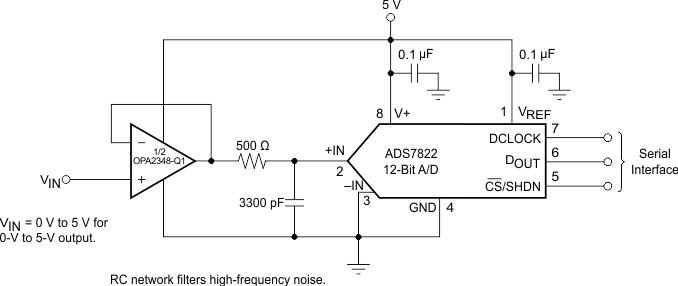
The OPAx348-Q1 op amps are optimized for driving medium-speed sampling ADCs. The OPAx348-Q1 op amps buffer the ADC input capacitance and resulting charge injection while providing signal gain.
Figure 26 shows the OPA2348 in a basic noninverting configuration driving the ADS7822 device. The ADS7822 device is a 12-bit, micropower sampling converter in the MSOP-8 package. When used with the low-power miniature packages of the OPAx348-Q1 family of devices, the combination is ideal for space-limited, low-power applications. In this configuration, an RC network at the ADC input can be used to provide for anti-aliasing filtering and charge injection current.
The OPAx348-Q1 family of devices can also be used in noninverting configuration to drive the ADS7822 device in limited low-power applications. In this configuration, an RC network at the ADC input can be used to provide for anti-aliasing filtering and charge injection current. See Figure 26 for the OPAx348-Q1 driving an ADS7822 device in a speech bandpass filtered data acquisition system. This small, low-cost solution provides the necessary amplification and signal conditioning to interface directly with an electret microphone. This circuit operates with VS = 2.7 V to 5 V with less than 250-µA typical quiescent current.
Some applications require differential signals. Figure 28 shows a simple circuit to convert a single-ended input of 0.1 V to 2.4 V into a differential output of ±2.3 V on a single 2.7-V supply. The output range is intentionally limited to maximize linearity. The circuit is composed of two amplifiers. One amplifier functions as a buffer and creates a voltage, VOUT+. The second amplifier inverts the input and adds a reference voltage to generate VOUT–. Both VOUT+ and VOUT– range from 0.1 V to 2.4 V. The difference, VDIFF, is the difference between VOUT+ and VOUT–. This configuration makes the differential output voltage range to be 2.3 V.
The design requirements are as follows:
The circuit in Figure 28 takes a single-ended input signal, VIN, and generates two output signals, VOUT+ and VOUT– using two amplifiers and a reference voltage, VREF. VOUT+ is the output of the first amplifier and is a buffered version of the input signal, VIN (as shown in Equation 1). VOUT– is the output of the second amplifier which uses VREF to add an offset voltage to VIN and feedback to add inverting gain. The transfer function for VOUT– is given in Equation 2.
The differential output signal, VDIFF, is the difference between the two single-ended output signals, VOUT+ and VOUT–. Equation 3 shows the transfer function for VDIFF. By applying the conditions that R1 = R2 and R3 = R4, the transfer function is simplified into Equation 6. Using this configuration, the maximum input signal is equal to the reference voltage and the maximum output of each amplifier is equal to VREF. The differential output range is 2 × VREF. Furthermore, the common-mode voltage (VCM) is one half of VREF (see Equation 7).
Linearity over the input range is key for good dc accuracy. The common-mode input range and output swing limitations determine the linearity. In general, an amplifier with rail-to-rail input and output swing is required. Bandwidth is a key concern for this design, so the OPAx348-Q1 family of devices is selected because its bandwidth is greater than the target of 1 MHz. The bandwidth and power ratio makes this device power-efficient, and the low offset and drift ensure good accuracy for moderate precision applications.
Because the transfer function of VOUT– relies heavily upon resistors (R1, R2, R3, and R4), use resistors with low tolerances to maximize performance and minimize error. This design uses resistors with resistance values of 49.9 kΩ and tolerances of 0.1%. However, if the noise of the system is a key parameter, smaller resistance values (6 kΩ or lower) can be selected to keep the overall system noise low. This technique ensures that the noise from the resistors is lower than the amplifier noise.
The OPAx348-Q1 family of devices is specified for operation from 1.8 V to 5.5 V (±0.9 V to ±2.75 V); many specifications apply from –40°C to 125°C. The Typical Characteristics presents parameters that can exhibit significant variance with regard to operating voltage or temperature.
CAUTION
Supply voltages larger than 7 V can permanently damage the device (see the Absolute Maximum Ratings).
Place 0.1-μF bypass capacitors close to the power-supply pins to reduce errors coupling in from noisy or high-impedance power supplies. For more detailed information on bypass capacitor placement, refer to the Layout Guidelines section.
For best operational performance of the device, use good PCB layout practices, including:
Table 1 lists quick access links. Categories include technical documents, support and community resources, tools and software, and quick access to sample or buy.
PARTS | PRODUCT FOLDER | SAMPLE & BUY | TECHNICAL DOCUMENTS | TOOLS & SOFTWARE | SUPPORT & COMMUNITY |
---|---|---|---|---|---|
OPA348-Q1 | Click here | Click here | Click here | Click here | Click here |
OPA2348-Q1 | Click here | Click here | Click here | Click here | Click here |
OPA4348-Q1 | Click here | Click here | Click here | Click here | Click here |
The following links connect to TI community resources. Linked contents are provided "AS IS" by the respective contributors. They do not constitute TI specifications and do not necessarily reflect TI's views; see TI's Terms of Use.
E2E is a trademark of Texas Instruments.
All other trademarks are the property of their respective owners.
These devices have limited built-in ESD protection. The leads should be shorted together or the device placed in conductive foam during storage or handling to prevent electrostatic damage to the MOS gates.
SLYZ022 — TI Glossary.
This glossary lists and explains terms, acronyms, and definitions.
The following pages include mechanical, packaging, and orderable information. This information is the most current data available for the designated devices. This data is subject to change without notice and revision of this document. For browser-based versions of this data sheet, refer to the left-hand navigation.
Texas Instruments Incorporated and its subsidiaries (TI) reserve the right to make corrections, enhancements, improvements and other changes to its semiconductor products and services per JESD46, latest issue, and to discontinue any product or service per JESD48, latest issue. Buyers should obtain the latest relevant information before placing orders and should verify that such information is current and complete. All semiconductor products (also referred to herein as "components") are sold subject to TI's terms and conditions of sale supplied at the time of order acknowledgment.
TI warrants performance of its components to the specifications applicable at the time of sale, in accordance with the warranty in TI's terms and conditions of sale of semiconductor products. Testing and other quality control techniques are used to the extent TI deems necessary to support this warranty. Except where mandated by applicable law, testing of all parameters of each component is not necessarily performed.
TI assumes no liability for applications assistance or the design of Buyers' products. Buyers are responsible for their products and applications using TI components. To minimize the risks associated with Buyers' products and applications, Buyers should provide adequate design and operating safeguards.
TI does not warrant or represent that any license, either express or implied, is granted under any patent right, copyright, mask work right, or other intellectual property right relating to any combination, machine, or process in which TI components or services are used. Information published by TI regarding third-party products or services does not constitute a license to use such products or services or a warranty or endorsement thereof. Use of such information may require a license from a third party under the patents or other intellectual property of the third party, or a license from TI under the patents or other intellectual property of TI.
Reproduction of significant portions of TI information in TI data books or data sheets is permissible only if reproduction is without alteration and is accompanied by all associated warranties, conditions, limitations, and notices. TI is not responsible or liable for such altered documentation. Information of third parties may be subject to additional restrictions.
Resale of TI components or services with statements different from or beyond the parameters stated by TI for that component or service voids all express and any implied warranties for the associated TI component or service and is an unfair and deceptive business practice. TI is not responsible or liable for any such statements.
Buyer acknowledges and agrees that it is solely responsible for compliance with all legal, regulatory and safety-related requirements concerning its products, and any use of TI components in its applications, notwithstanding any applications-related information or support that may be provided by TI. Buyer represents and agrees that it has all the necessary expertise to create and implement safeguards which anticipate dangerous consequences of failures, monitor failures and their consequences, lessen the likelihood of failures that might cause harm and take appropriate remedial actions. Buyer will fully indemnify TI and its representatives against any damages arising out of the use of any TI components in safety-critical applications.
In some cases, TI components may be promoted specifically to facilitate safety-related applications. With such components, TI's goal is to help enable customers to design and create their own end-product solutions that meet applicable functional safety standards and requirements. Nonetheless, such components are subject to these terms.
No TI components are authorized for use in FDA Class III (or similar life-critical medical equipment) unless authorized officers of the parties have executed a special agreement specifically governing such use.
Only those TI components which TI has specifically designated as military grade or "enhanced plastic" are designed and intended for use in military/aerospace applications or environments. Buyer acknowledges and agrees that any military or aerospace use of TI components which have not been so designated is solely at the Buyer's risk, and that Buyer is solely responsible for compliance with all legal and regulatory requirements in connection with such use.
TI has specifically designated certain components as meeting ISO/TS16949 requirements, mainly for automotive use. In any case of use of non-designated products, TI will not be responsible for any failure to meet ISO/TS16949.
TI E2E Community : e2e.ti.com
Mailing Address: Texas Instruments, Post Office Box 655303, Dallas, Texas 75265
Copyright© 2014, Texas Instruments Incorporated