-
SN65LVDx10x Differential Translator/Repeater SLLS516E August 2002 – July 2015 SN65LVDS100 , SN65LVDS101 , SN65LVDT100 , SN65LVDT101
UNLESS OTHERWISE NOTED, this document contains PRODUCTION DATA.
-
SN65LVDx10x Differential Translator/Repeater
- 1 Features
- 2 Applications
- 3 Description
- 4 Revision History
- 5 Description (Continued)
- 6 Device Options
- 7 Pin Configuration and Functions
- 8 Specifications
- 9 Parameter Measurement Information
- 10Detailed Description
-
11Application and Implementation
- 11.1 Application Information
- 11.2
Typical Application
- 11.2.1 PECL to LVDS Translation
- 11.2.2 LVDS to 3.3-V PECL Translation
- 11.2.3 5-V PECL to 3.3-V PECL Translation
- 11.2.4 CML to LVDS or 3.3-V PECL Translation
- 11.2.5 Single-Ended 3.3-V PECL to LVDS Translation
- 11.2.6 Single-Ended CMOS to LVDS Translation
- 11.2.7 Single-Ended CMOS to 3.3-V PECL Translation
- 11.2.8 Receipt of AC-Coupled Signals
- 12Power Supply Recommendations
- 13Layout
- 14Device and Documentation Support
- 15Mechanical, Packaging, and Orderable Information
- IMPORTANT NOTICE
パッケージ・オプション
デバイスごとのパッケージ図は、PDF版データシートをご参照ください。
メカニカル・データ(パッケージ|ピン)
- D|8
- DGK|8
サーマルパッド・メカニカル・データ
発注情報
SN65LVDx10x Differential Translator/Repeater
1 Features
- Designed for Signaling Rates ≥ 2 Gbps
- Total Jitter < 65 ps
- Low-Power Alternative for the MC100EP16
- Low 100-ps (Maximum) Part-to-Part Skew
- 25 mV of Receiver Input Threshold Hysteresis
Over 0-V to 4-V Input Voltage Range - Inputs Electrically Compatible With LVPECL,
CML, and LVDS Signal Levels - 3.3-V Supply Operation
- LVDT Integrates 110-Ω Terminating Resistor
- Offered in SOIC and MSOP
2 Applications
- Wireless Infrastructure
- Telecom Infrastructure
- Printers
3 Description
The SN65LVDS100, SN65LVDT100, SN65LVDS101, and SN65LVDT101 are high-speed differential receivers and drivers connected as repeaters. The receiver accepts low-voltage differential signaling (LVDS), positive-emitter-coupled logic (PECL), or current-mode logic (CML) input signals at rates up to 2 Gbps and repeats it as either an LVDS or PECL output signal. The signal path through the device is differential for low radiated emissions and minimal added jitter.
Device Information(1)
| PART NUMBER | PACKAGE | BODY SIZE (NOM) |
|---|---|---|
| SN65LVDS100 | SOIC (8) | 4.90 mm × 3.91 mm |
| VSSOP (8) | 3.00 mm × 3.00 mm | |
| SN65LVDT100 | SOIC (8) | 4.90 mm × 3.91 mm |
| VSSOP (8) | 3.00 mm × 3.00 mm | |
| SN65LVDS101 | SOIC (8) | 4.90 mm × 3.91 mm |
| VSSOP (8) | 3.00 mm × 3.00 mm | |
| SN65LVDT101 | SOIC (8) | 4.90 mm × 3.91 mm |
| VSSOP (8) | 3.00 mm × 3.00 mm |
- For all available packages, see the orderable addendum at the end of the data sheet.
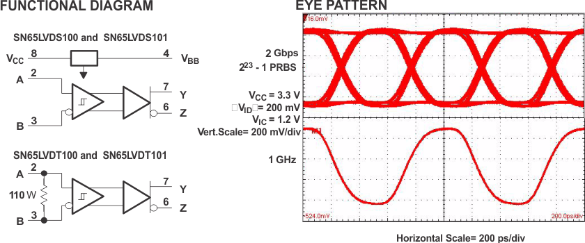
Dual Eye Diagram

4 Revision History
Changes from D Revision (December 2014) to E Revision
- Changed Features From: "Over 0-V to 4-V Common-Mode Range" To: "Over 0-V to 4-V Input Voltage Range"Go
Changes from C Revision (June 2004) to D Revision
- Added Pin Configuration and Functions section, ESD Ratings table, Feature Description section, Device Functional Modes, Application and Implementation section, Power Supply Recommendations section, Layout section, Device and Documentation Support section, and Mechanical, Packaging, and Orderable Information section Go
5 Description (Continued)
The outputs of the SN65LVDS100 and SN65LVDT100 are LVDS levels as defined by TIA/EIA-644-A. The outputs of the SN65LVDS101 and SN65LVDT101 are compatible with 3.3-V PECL levels. Both drive differential transmission lines with nominally 100-Ω characteristic impedance.
The SN65LVDT100 and SN65LVDT101 include a 110-Ω differential line termination resistor for less board space, fewer components, and the shortest stub length possible. They do not include the VBB voltage reference found in the SN65LVDS100 and SN65LVDS101. VBB provides a voltage reference of typically 1.35 V below VCC for use in receiving single-ended input signals and is particularly useful with single-ended 3.3-V PECL inputs. When VBB is not used, it should be unconnected or open.
All devices are characterized for operation from –40°C to 85°C.
6 Device Options
| ORDERABLE PART NUMBER | OUTPUT | TERMINATION RESISTOR | VBB |
|---|---|---|---|
| SN65LVDS100D | LVDS | No | Yes |
| SN65LVDS100DGK | LVDS | No | Yes |
| SN65LVDT100D | LVDS | Yes | No |
| SN65LVDT100DGK | LVDS | Yes | No |
| SN65LVDS101D | LVPECL | No | Yes |
| SN65LVDS101DGK | LVPECL | No | Yes |
| SN65LVDT101D | LVPECL | Yes | No |
| SN65LVDT101DGK | LVPECL | Yes | No |
7 Pin Configuration and Functions

Pin Functions
| PIN | I/O | DESCRIPTION | ||
|---|---|---|---|---|
| NAME | SN65LVDS100, SN65LVDS101 | SN65LVDT100, SN65LVDT101 | ||
| A | 2 | 2 | I | Differential non-inverting input |
| B | 3 | 3 | I | Differential inverting input |
| GND | 5 | 5 | — | Ground |
| NC | 1 | 1, 4 | — | No connect |
| VBB | 4 | — | O | Voltage reference |
| VCC | 8 | 8 | — | Supply voltage |
| Y | 7 | 7 | O | Differential non-inverting output |
| Z | 6 | 6 | O | Differential inverting output |