SCES656E February 2006 – November 2016 SN74LV4046A
PRODUCTION DATA.
- 1 Features
- 2 Applications
- 3 Description
- 4 Revision History
- 5 Pin Configuration and Functions
- 6 Specifications
- 7 Detailed Description
- 8 Application and Implementation
- 9 Power Supply Recommendations
- 10Layout
- 11Device and Documentation Support
- 12Mechanical, Packaging, and Orderable Information
パッケージ・オプション
メカニカル・データ(パッケージ|ピン)
サーマルパッド・メカニカル・データ
発注情報
1 Features
- ESD Protection Exceeds JESD 22
- 2000-V Human Body Model (A114-A)
- 1000-V Charged-Device Model (C101)
- Choice of Three Phase Comparators
- Exclusive OR
- Edge-Triggered J-K Flip-Flop
- Edge-Triggered RS Flip-Flop
- Excellent VCO Frequency Linearity
- VCO-Inhibit Control for ON/OFF Keying and for Low Standby Power Consumption
- Optimized Power-Supply Voltage Range From
3 V to 5.5 V - Wide Operating Temperature Range From
–40°C to +125°C - Latch-Up Performance Exceeds 250 mA Per JESD 17
2 Applications
- Telecommunications
- Signal Generators
- Digital Phase-Locked Loop
3 Description
The SN74LV4046A is a high-speed silicon-gate CMOS device that is pin compatible with the CD4046B and the CD74HC4046. The device is specified in compliance with JEDEC Std 7.
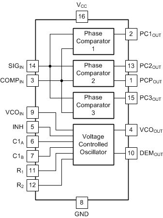
The SN74LV4046A is a phase-locked loop (PLL) circuit that contains a linear voltage-controlled oscillator (VCO) and three different phase comparators (PC1, PC2, and PC3). A signal input and a comparator input are common to each comparator.
The signal input can be directly coupled to large voltage signals, or indirectly coupled (with a series capacitor) to small voltage signals. A self-bias input circuit keeps small voltage signals within the linear region of the input amplifiers. With a passive low-pass filter, the SN74LV4046A forms a second-order loop PLL. The excellent VCO linearity is achieved by the use of linear operational amplifier techniques. Various applications include telecommunications, digital phase-locked loop and signal generators.
Device Information(1)
| PART NUMBER | PACKAGE | BODY SIZE (NOM) |
|---|---|---|
| SN74LV4046ANS | SO (16) | 7.70 mm × 10.20 mm |
| SN74LV4046AD | SOIC (16) | 6.00 mm × 9.90 mm |
| SN74LV4046APW | TSSOP (16) | 6.40 mm × 5.00 mm |
| SN74LV4046ADGVR | TVSOP (16) | 3.60 mm × 4.40 mm |
| SN74LV4046AN | PDIP (16) | 19.30 mm × 6.35 mm |
- For all available packages, see the orderable addendum at the end of the data sheet.
SN74LV4046A Functional Block Diagram

4 Revision History
Changes from D Revision (September 2015) to E Revision
- Deleted 200-V Machine Model (A115-A) from FeaturesGo
- Added TVSOP and PDIP packages to Device Information tableGo
- Added TVSOP, SO, and PDIP packages to pinoutGo
- Changed RθJA for D package from 73°C/W to 82.8°C/WGo
- Changed RθJA for DGV package from 120°C/W to 116.8°C/WGo
- Changed RθJA for NS package from 64°C/W to 83.5°C/WGo
- Changed RθJA for PW package from 108°C/W to 108.1°C/WGo
- Added values in the Thermal Information table to align with JEDEC standards Go
- Changed x-axis from "–360° 0° 360°" to "0° 90° 180°" Go
- Changed "(VCC/4)" to "(VCC/4π)"Go
- Added Receiving Notification of Documentation Updates sectionGo
Changes from C Revision (April 2007) to D Revision
- Added Pin Configuration and Functions section, ESD Ratings table, Feature Description section, Device Functional Modes, Application and Implementation section, Power Supply Recommendations section, Layout section, Device and Documentation Support section, and Mechanical, Packaging, and Orderable Information section Go