-
TLK10xL Industrial Temp, Single Port 10/100Mbs Ethernet Physical Layer Transceiver
- 1Device Overview
- 2Revision History
- 3Pin Configuration and Functions
-
4Specifications
- 4.1 Absolute Maximum Ratings
- 4.2 ESD Ratings
- 4.3 Recommended Operating Conditions
- 4.4 20
- 4.5 TLK106L 32-Pin Extended Temperature (105°C) Device Thermal Characteristics
- 4.6 DC Characteristics, VDD_IO
- 4.7 DC Characteristics
- 4.8 Power Supply Characteristics
- 4.9
AC Specifications
- 4.9.1 Power Up Timing
- 4.9.2 Reset Timing
- 4.9.3 MII Serial Management Timing
- 4.9.4 100Mb/s MII Transmit Timing
- 4.9.5 100Mb/s MII Receive Timing
- 4.9.6 100Base-TX Transmit Packet Latency Timing
- 4.9.7 100Base-TX Transmit Packet Deassertion Timing
- 4.9.8 100Base-TX Transmit Timing (tR/F and Jitter)
- 4.9.9 100Base-TX Receive Packet Latency Timing
- 4.9.10 100Base-TX Receive Packet Deassertion Timing
- 4.9.11 10Mbs MII Transmit Timing
- 4.9.12 10Mb/s MII Receive Timing
- 4.9.13 10Base-T Transmit Timing (Start of Packet)
- 4.9.14 10Base-T Transmit Timing (End of Packet)
- 4.9.15 10Base-T Receive Timing (Start of Packet)
- 4.9.16 10Base-T Receive Timing (End of Packet)
- 4.9.17 10Mb/s Jabber Timing
- 4.9.18 10Base-T Normal Link Pulse Timing
- 4.9.19 Auto-Negotiation Fast Link Pulse (FLP) Timing
- 4.9.20 100Base-TX Signal Detect Timing
- 4.9.21 100Mbs Loopback Timing
- 4.9.22 10Mbs Internal Loopback Timing
- 4.9.23 RMII Transmit Timing
- 4.9.24 RMII Receive Timing
- 4.9.25 Isolation Timing
-
5Detailed Description
- 5.1 Hardware Configuration
- 5.2
Architecture
- 5.2.1 100Base-TX Transmit Path
- 5.2.2
100Base-TX Receive Path
- 5.2.2.1 Analog Front End
- 5.2.2.2 Adaptive Equalizer
- 5.2.2.3 Baseline Wander Correction
- 5.2.2.4 NRZI and MLT-3 Decoding
- 5.2.2.5 Descrambler
- 5.2.2.6 5B/4B Decoder and Nibble Alignment
- 5.2.2.7 Timing Loop and Clock Recovery
- 5.2.2.8 Phase-Locked Loops (PLL)
- 5.2.2.9 Link Monitor
- 5.2.2.10 Signal Detect
- 5.2.2.11 Bad SSD Detection
- 5.2.3 10Base-T Receive Path
- 5.2.4 Auto Negotiation
- 5.2.5 Link Down Functionality
- 5.2.6 IEEE 1588 Precision Timing Protocol Support
- 5.3
Register Maps
- 5.3.1
Register Definition
- 5.3.1.1 Basic Mode Control Register (BMCR)
- 5.3.1.2 Basic Mode Status Register (BMSR)
- 5.3.1.3 PHY Identifier Register 1 (PHYIDR1)
- 5.3.1.4 PHY Identifier Register 2 (PHYIDR2)
- 5.3.1.5 Auto-Negotiation Advertisement Register (ANAR)
- 5.3.1.6 Auto-Negotiation Link Partner Ability Register (ANLPAR) (BASE Page)
- 5.3.1.7 Auto-Negotiate Expansion Register (ANER)
- 5.3.1.8 Auto-Negotiate Next Page Transmit Register (ANNPTR)
- 5.3.1.9 Auto-Negotiation Link Partner Ability Next Page Register (ANLNPTR)
- 5.3.1.10 Control register 1 (CR1)
- 5.3.1.11 Control register 2 (CR2)
- 5.3.1.12 Control Register 3 (CR3)
- 5.3.1.13 Extended Register Addressing
- 5.3.1.14 Fast Link Down Status Register
- 5.3.1.15 PHY Status Register (PHYSTS)
- 5.3.1.16 PHY Specific Control Register (PHYSCR)
- 5.3.1.17 MII Interrupt Status Register 1 (MISR1)
- 5.3.1.18 MII Interrupt Status Register 2 (MISR2)
- 5.3.1.19 False Carrier Sense Counter Register (FCSCR)
- 5.3.1.20 Receiver Error Counter Register (RECR)
- 5.3.1.21 BIST Control Register (BISCR)
- 5.3.1.22 RMII Control and Status Register (RCSR)
- 5.3.1.23 LED Control Register (LEDCR)
- 5.3.1.24 PHY Control Register (PHYCR)
- 5.3.1.25 10Base-T Status/Control Register (10BTSCR)
- 5.3.1.26 BIST Control and Status Register 1 (BICSR1)
- 5.3.1.27 BIST Control and Status Register2 (BICSR2)
- 5.3.2 Cable Diagnostic Control Register (CDCR)
- 5.3.3 PHY Reset Control Register (PHYRCR)
- 5.3.4 Multi LED Control register (MLEDCR)
- 5.3.5 Compliance Test register (COMPTR)
- 5.3.6 IEEE1588 Precision Timing Pin Select (PTPPSEL)
- 5.3.7 IEEE1588 Precision Timing Configuration (PTPCFG)
- 5.3.8 TX_CLK Phase Shift Register (TXCPSR)
- 5.3.9 Power Back Off Control Register (PWRBOCR)
- 5.3.10 Voltage Regulator Control Register (VRCR)
- 5.3.11
Cable Diagnostic Configuration/Result Registers
- 5.3.11.1 ALCD Control and Results 1 (ALCDRR1)
- 5.3.11.2 Cable Diagnostic Specific Control Registers (CDSCR1 - CDSCR4)
- 5.3.11.3 Cable Diagnostic Location Results Register 1 (CDLRR1)
- 5.3.11.4 Cable Diagnostic Location Results Register 2 (CDLRR2)
- 5.3.11.5 Cable Diagnostic Location Results Register 3 (DDLRR3)
- 5.3.11.6 Cable Diagnostic Location Results Register 4 (CDLRR4)
- 5.3.11.7 Cable Diagnostic Location Results Register 5 (CDLRR5)
- 5.3.11.8 Cable Diagnostic Amplitude Results Register 1 (CDARR1)
- 5.3.11.9 Cable Diagnostic Amplitude Results Register 2 (CDARR2)
- 5.3.11.10 Cable Diagnostic Amplitude Results Register 3 (CDARR3)
- 5.3.11.11 Cable Diagnostic Amplitude Results Register 4 (CDARR4)
- 5.3.11.12 Cable Diagnostic Amplitude Results Register 5 (CDARR5)
- 5.3.11.13 Cable Diagnostic General Results Register (CDGRR)
- 5.3.11.14 ALCD Control and Results 2 (ALCDRR2)
- 5.3.11.15 ALCD Control and Results 3 (ALCDRR3)
- 5.3.1
Register Definition
- 6Applications, Implementation, and Layout
- 7Device and Documentation Support
- 8Mechanical Packaging and Orderable Information
- IMPORTANT NOTICE
パッケージ・オプション
メカニカル・データ(パッケージ|ピン)
- RHB|32
サーマルパッド・メカニカル・データ
- RHB|32
発注情報
TLK10xL Industrial Temp, Single Port 10/100Mbs Ethernet Physical Layer Transceiver
1 Device Overview
1.1 Features
- Low-Power Consumption:
- Single Supply: <205 mW PHY, 275 mW With Center Tap (Typical)
- Dual Supplies: <126 mW PHY, 200 mW With Center Tap (Typical)
- Programmable Power Back Off to Reduce PHY Power up to 20% in Systems With Shorter Cables
- IEEE 1588 SFD Indication Enables Time Stamping by a Controller or Processor
- Low Deterministic Latency Supports IEEE1588 Implementation
- Cable Diagnostics
- Programmable Fast Link Down Modes, <10 µs Reaction Time
- Variable I/O voltage range: 3.3V, 2.5V, 1.8V
- MAC Interface I/O voltage range:
- MII I/O voltage range: 3.3V, 2.5V, 1.8V
- RMII I/O voltage range: 3.3V, 2.5V
- Fixed TX Clock to XI, With Programmable Phase Shift
- Auto-MDIX for 10/100Mbs
- Energy Detection Mode
- MII and RMII Capabilities
- IEEE 802.3u MII
- Error-Free 100Base-T Operation up to 150 Meters Under Typical Conditions
- Error-Free 10Base-T Operation up to 300 Meters Under Typical Conditions
- Serial Management Interface
- IEEE 802.3u Auto-Negotiation and Parallel Detection
- IEEE 802.3u ENDEC, 10Base-T Transceivers and Filters
- IEEE 802.3u PCS, 100Base-TX Transceivers
- Integrated ANSI X3.263 Compliant TP-PMD Physical Sublayer with Adaptive Equalization and Baseline Wander Compensation
- Programmable LED Support Link, Activity
- 10/100Mbs Packet BIST (Built in Self Test)
- HBM ESD Protection on RD± and TD± of 16 kV
- 32-pin VQFN (5 mm) × (5 mm)
1.2 Applications
- Industrial Networks and Factory Automation
- Motor and Motion Control
- General Embedded Applications
1.3 Description
The TLK10xL is a single-port Ethernet PHY for 10Base-T and 100Base TX signaling, integrating all the physical-layer functions needed to transmit and receive data on standard twisted-pair cables. The device supports the standard Media Independent Interface (MII) and Reduced Media Independent Interface (RMII) for direct connection to a Media Access Controller (MAC).
The device is designed for power-supply flexibility, and can operate with a single 3.3-V power supply or with combinations of 3.3-V and 1.55-V power supplies for reduced power operation.
The TLK10xL uses mixed-signal processing to perform equalization, data recovery, and error correction to achieve robust operation over CAT 5 twisted-pair wiring. The TLK10xL not only meets the requirements of IEEE 802.3, but maintains high margins in terms of cross-talk and alien noise.
The TLK10xL Ethernet PHY has a special Power Back Off mode to conserve power in systems with relatively short cables. This mode provides the flexibility to reduce system power when the system is not required to drive the standard IEEE 802.3 100-m cable length, or the extended 150m, error-free cable reach of the TLK10xL. For more detail, see application note SLLA328.

1.4 Functional Block Diagram
 Figure 1-1 TLK10xL Functional Block Diagram
2 Revision History
Changes from C Revision (November 2014) to D Revision
- Changed description of I/O Voltage Range and MAC interfaces to clarify voltages. Go
- Changed QFN to VQFN Go
- Added package informationGo
- Added note for oscillator voltage levelsGo
- Updated Handling Ratings to ESD Ratings and moved Storage temperature to Absolute Maximum RatingsGo
- Added parameters for dual-supply operationGo
- Changed Thermal Table format Go
- Added timing parameter for XI clock stability after power up. Go
- Deleted CLK25MHz_OUTGo
- Added note on impact of enabling Enhanced LED link on link blinkingGo
- Changed format of table header. Go
- Added note that the default transmit link pulse polarity is reversedGo
- Changed Register Block to Register Maps Go
- Added Compliance Test register. Go
- Changed format of Register Table header row. Go
- Changed VRCR bits 3:0 to RESERVED. Go
- Changed Speed Selection register bit to RWGo
- Changed Auto-Negotiation Enable register bit to RWGo
- Added Reserved bitsGo
- Added note that enabling Enhanced LED Link overrides the LED blinking functionality of PHYCR register bit 5Go
- Changed default to inverted polarity Go
- Added text in MLEDCR clarifying polarity of LED. Go
- Added Compliance Test register, address 0x0027 Go
- Changed Power Back Off Levels Go
- Changed VRCR bits 3:0 to RESERVED Go
- Changed "the same levels as the MII interface" to "operates at 3.3V or 2.5V VDD_IO levels" Go
- Deleted partial list of recommended transformers Go
- Changed recommendation for common mode chokes to requirement. Go
- Deleted the amplitude of the oscillator should be a nominal voltage of 3.3V. Go
- Added notes on oscillator supply voltage.Go
Changes from B Revision (January 2014) to C Revision
- Deleted "(TLK106)"Go
- Deleted "IEEE 802.3u 100BASE-FX Fiber Interface"Go
- Deleted "Additionally, the TLK10xL supports 100Base-FX signaling via an external optical transceiver."Go
- Deleted "SD_IN"Go
- Deleted Redundant row "Power dissipation 200 mW"Go
- Deleted DC Characteristics, SD_INGo
- VTH1 - max value deleted, 200-mV typ value addedGo
- Deleted FX TimingGo
- Deleted 25MHz_OUT Clock TimingGo
- Deleted FIBCR RegisterGo
- Deleted Fiber Mode Control 2 and Fiber Mode Control 3Go
- Deleted Fiber Mode ControlGo
- Deleted Fiber Mode Control Register, Fiber Mode Control 2 and Fiber Mode Control 3Go
- Deleted Bit[14] Fiber Mode ControlGo
- Changed "Active WOL" to "Active Energy Saving"Go
- Changed "Passive WOL" to "Passive Energy Saving"Go
- Changed "1" to "0"Go
- Deleted Fiber Mode Control Register (FIBCR)Go
- Deleted Fiber Mode Control Register 2 (FIBCR2)Go
- Deleted Fiber Mode Control Register 3 (FIBCR3)Go
- Changed "WOL (Wake-On LAN)" to "Energy Saving"Go
- Changed "WOL (Wake-On LAN)" to "Energy Saving"Go
Changes from A Revision (November 2013) to B Revision
- Changed "Low Power Consumption: <205mW PHY and 275mW with Center Tap (Typical)" to "Low Power Consumption: <126mW PHY and 200mW with Center Tap (Typical, dual supplies)"Go
- Changed "MII and RMII Interfaces" to "MII and RMII Capabilities"Go
- Changed "Error-Free Operation up to 150 Meters Under Typical Conditions" to "Error-Free 100Base-T Operation up to 150 Meters Under Typical Conditions Error-Free 10Base-T Operation up to 300 Meters Under Typical Conditions"Go
- Added operating conditions for single and dual suppliesGo
- Changed title from "Active Power" to "Active Power, Single Supply Operation"Go
- Added Dual Supply Operation tableGo
- Added bit 10, Fast Link Down Mode enable, Drop the link based on descrambler link loss, adusted description of bits 3:0 to reflect 5 options instead of 4Go
- Deleted " Allow the system to reset the PHY using register access."Go
- Changed recommended transformer from Pulse HX1188 to Pulse HX1198Go
Changes from * Revision (August 2013) to A Revision
- Updated Pin Layout, changed "VDD33_IO" to "VDD_IO"Go
- Added maximum storage temperatureGo
- Changed "... stable for minimum of 1ms ..." to "... stable for minimum of 1µs ..." (typo correction)Go
- Changed titles, "100Base-TX ... Timing" to "100Base-TX / FX ... Timing"Go
- Added Power Back Off Control Register (0AEh)Go
- Registers 0010h - 001Fh moved from extended-addressing space to direct-addressing spaceGo
- Changed default value for MDL_REV from 0001 to 0010Go
- Changed Default value of interrupt-polarity bit from 0 to 1 Go
- Updated RMII Control and Status Register bit 4 descriptionGo
3 Pin Configuration and Functions
The TLK10xL pins fall into the following interface categories (subsequent sections describe each interface):
|
|
Note: Configuration pin option. See Section 5.1.1 for Jumper Definitions.
The definitions below define the functionality of each pin.
| Type: I | Input | Type: OD | Open Drain | |
| Type: O | Output | Type: PD, PU | Internal Pulldown/Pullup | |
| Type: I/O | Input/Output | Type: S | Configuration Pin (All configuration pins have weak internal pullups or pulldowns. Use an external 2.2kΩ resistor if you need a different default value. See Section 5.1.1 for details.) |
3.1 Pin Diagram
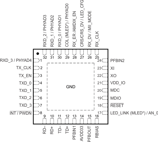
This document describes signals that take on different names depending on configuration. In such cases, the different names are placed together and separated by slash (/) characters. For example, "RXD_3 / PHYAD4". Active-low signals are represented by overbars.
.
.
.
3.2 Serial Management Interface (SMI)
| PIN | TYPE | DESCRIPTION | |
|---|---|---|---|
| NAME | NO. | ||
| MDC | 20 | I | MANAGEMENT DATA CLOCK: Clock signal for the management data input/output (MDIO) interface. The maximum MDC rate is 25MHz; there is no minimum MDC rate. MDC is not required to be synchronous to the TX_CLK or the RX_CLK. |
| MDIO | 19 | I/O | MANAGEMENT DATA I/O: Bidirectional command / data signal synchronized to MDC. Either the local controller or the TLK10xL may drive the MDIO signal. This pin requires a pull-up resistor with value 2.2kΩ. |
3.3 MAC Data Interface
| PIN | TYPE | DESCRIPTION | |
|---|---|---|---|
| NAME | NO. | ||
| TX_CLK | 2 | O, PD |
MII TRANSMIT CLOCK: MII Transmit Clock provides the 25MHz or 2.5MHz reference clock depending on the speed. Note that in MII mode, this clock has constant phase referenced to REF_CLK. Applications requiring such constant phase may use this feature. Unused in RMII mode. In RMII, X1 reference clock is used as the clock for both transmit and receive. |
| TX_EN | 3 | I, PD | TRANSMIT ENABLE: TX_EN is presented on the rising edge of the TX_CLK . TX_EN indicates the presence of valid data inputs on TXD[3:0] in MII mode, and on TXD [1:0] in the RMII mode. TX_EN is an active high signal. |
| TXD_0 TXD_1 TXD_2 TXD_3 |
4
5 6 7 |
I, PD | TRANSMIT DATA: In MII mode, the transmit data nibble received from the MAC is synchronous to the rising edge of the TX_CLK signal. In RMII mode, TXD [1:0] received from the MAC is synchronous to the 50MHz reference clock on XI. |
| RX_CLK | 25 | O | RECEIVE CLOCK: In MII mode it is the receive clock that provides either a 25MHz or 2.5MHz reference clock, depending on the speed, that is derived from the received data stream. |
| RX_DV / MII_MODE | 26 | S, O, PD | RECEIVE DATA VALID: This pin indicates valid data is present on the RXD [3:0] for MII mode or on RXD [1:0] for RMII mode, independently from Carrier Sense. |
| RX_ER / AMDIX_EN | 28 | S, O, PU | RECEIVE ERROR: This pin indicates that an error symbol has been detected within a received packet in both MII and RMII mode. In MII mode, RX_ER is asserted high synchronously to RX_CLK and in RMII mode, synchronously to XI (50MHz). This pin is not required to be used by the MAC, in either MII or RMII, because the PHY is corrupting data on a receive error. |
| RXD_0 / PHYAD1 RXD_1 / PHYAD2 RXD_2 / PHYAD3 RXD_3 / PHYAD4 |
30
31 32 1 |
S, O, PD | RECEIVE DATA: Symbols received on the cable are decoded and presented on these pins synchronous to RX_CLK. They contain valid data when RX_DV is asserted. A nibble RXD [3:0] is received in the MII mode and 2-bits RXD[1:0] is received in the RMII Mode. PHY address pins PHYAD[4:1] are multiplexed with RXD [3:0], and are pulled down. PHYAD0 (LSB of the address) is multiplexed with COL on pin 29, and is pulled up. If no external pullup/pulldown is present, the default address is 0x01. |
| CRS / CRS_DV/ LED_CFG | 27 | S, O, PU |
CARRIER SENSE: In MII mode this pin is asserted high when the receive medium is non-idle. CARRIER SENSE/RECEIVE DATA VALID: In RMII mode, this pin combines the RMII Carrier and Receive Data Valid indications. |
| COL (MLED)/ PHYAD0 | 29 | S, O, PU |
COLLISION DETECT: For MII mode in Full Duplex Mode this pin is always low. In 10Base-T/100Base-TX half-duplex modes, this pin is asserted HIGH only when both transmit and receive media are non-idle. This pin is not used in RMII mode. MLED: The Multi LED can be routed to this pin via REG 0x0025 (MLEDCR Register), for further details see Section 5.1.8. |
3.4 10Mbs and 100Mbs PMD Interface
| PIN | TYPE | DESCRIPTION | |
|---|---|---|---|
| NAME | NO. | ||
| TD–, TD+ | 11, 12 | I/O | Differential common driver transmit output (PMD Output Pair): These differential outputs are automatically configured to either 10Base-T or 100Base-TX signaling. In Auto-MDIX mode of operation, this pair can be used as the Receive Input pair. These pins require 3.3V bias for operation. |
| RD–, RD+ | 9, 10 | I/O | Differential receive input (PMD Input Pair): These differential inputs are automatically configured to accept either 100Base-TX or 10Base-T signaling. In Auto-MDIX mode of operation, this pair can be used as the Transmit Output pair. These pins require 3.3V bias for operation. |
3.5 Clock Interface
3.6 LED Interface
(See Table 5-4 and Table 5-5 for LED Mode Selection)| PIN | TYPE | DESCRIPTION | ||
|---|---|---|---|---|
| NAME | NO. | |||
| LED_LINK (MLED(1)) / AN_0 | 17 | S, O, PU | LED Pin to indicate status | |
| Mode 1 | LINK Indication LED: Indicates the status of the link. When the link is good, the LED is ON. | |||
| Mode 2 | ACT indication LED: Indicates transmit and receive activity in addition to the status of the Link. The LED is ON when Link is good. The LED blinks when the transmitter or receiver is active. | |||
3.7 Reset and Power Down
| PIN | TYPE | DESCRIPTION | |
|---|---|---|---|
| NAME | NO. | ||
| RESET | 18 | I, PU | This pin is an active-low reset input that initializes or re-initializes all the internal registers of the TLK10xL. Asserting this pin low for at least 1µs will force a reset process to occur. All jumper options are reinitialized as well. |
| INT / PWDN | 8 | IO, OD, PU | Register access is required for this pin to be configured either as power down or as an interrupt. The default function of this pin is power down. |
| When this pin is configured for a power down function, an active low signal on this pin places the device in power down mode. | |||
| When this pin is configured as an interrupt pin, then this pin is asserted low when an interrupt condition occurs. The pin has an open-drain output with a weak internal pull-up. Some applications may require an external pull-up resistor. | |||
3.8 Power and Bias Connections
| PIN | TYPE | DESCRIPTION | |
|---|---|---|---|
| NAME | NO. | ||
| RBIAS | 16 | I | Bias Resistor Connection: Use a 4.87kΩ 1% resistor connected from RBIAS to GND. |
| PFBOUT | 15 | O | Power Feedback Output: Place 10µf and 0.1μF capacitors (ceramic preferred) close to PFBOUT. |
| In single-supply operation, connect this pin to PFBIN1 and PFBIN2 (pin 13 and pin 24). See Figure 5-1 for proper placement. | |||
| In multiple supply operation, this pin is not used. | |||
| PFBIN1 | 13 | I | Power Feedback Input: These pins are fed with power from PFBOUT (pin 15) in single supply operation. |
| PFBIN2 | 24 | In multiple supply operation, connect a 1.55V external power supply to these pins. Connect a small capacitor of 0.1µF close to each pin. To power down the internal linear regulator, write to register 0x00d0. | |
| VDD_IO | 21 | P | I/O 3.3V, 2.5V, or 1.8V Supply - For details, see Section 5.1.2.3 |
| AVDD33 | 14 | P | Analog 3.3V power supply |
| GND | Ground Pad | P | Ground Pad |
4 Specifications
All parameters are derived by test, statistical analysis, or design.
4.1 Absolute Maximum Ratings(1)
| MIN | MAX | UNIT | |||
|---|---|---|---|---|---|
| VDD_IO, AVDD33 | Supply voltage | –0.3 | 3.8 | V | |
| PFBIN1, PFBIN2 | –0.3 | 1.8 | |||
| XI | DC Input voltage | –0.3 | 3.8 | V | |
| TD-, TD+, RD-, RD+ | –0.3 | 6 | |||
| Other Inputs | –0.3 | 3.8 | |||
| XO | DC Output voltage | –0.3 | 3.8 | V | |
| Other outputs | –0.3 | 3.8 | |||
| TJ | Maximum die temperature | 125 | °C | ||
| Tstg | Storage temperature | –65 | 150 | °C | |
4.2 ESD Ratings
| VALUE | UNIT | ||||
|---|---|---|---|---|---|
| VESD | Electrostatic discharge (ESD) performance: | Human Body Model (HBM), per ANSI/ESDA/JEDEC JS001(1) | All pins(3) | ±4000 | V |
| Ethernet network pins (TD+, TD–, RD+, RD–)(5) | ±16000 | ||||
| Charged Device Model (CDM), per JESD22-C101(2) |
All pins(4) | ±750 | V | ||
4.3 Recommended Operating Conditions
| MIN | NOM | MAX | UNIT | |||
|---|---|---|---|---|---|---|
| DUAL SUPPLY OPERATION | ||||||
| Core Supply voltage (PFBIN1, PFBIN2) | 1.48 | 1.55 | 1.68 | V | ||
| PD | Power dissipation(2) | 200 | mW | |||
| SINGLE SUPPLY OPERATION | ||||||
| (PFBOUT connected to PFBIN1, PFBIN2 See Figure 5-1) | ||||||
| PD | Power dissipation(1) | 270 | mW | |||
| AVDD33 | Analog 3.3-V Supply | 3.0 | 3.3 | 3.6 | V | |
| VDD_IO | 3.3-V Option | 3.0 | 3.3 | 3.6 | V | |
| 2.5-V Option | 2.25 | 2.5 | 2.75 | |||
| 1.8-V Option (MII Mode only) | 1.62 | 1.8 | 1.98 | |||
| TA | Ambient temperature(3) | TLK105L | –40 | 85 | °C | |
| TLK106L | –40 | 105 | ||||
4.4
4.4.1 TLK105L 32-Pin Industrial Device (85°C) Thermal Characteristics
over operating free-air temperature range (unless otherwise noted)| THERMAL METRIC(1) | TLK105L, TLK106L | UNIT | |
|---|---|---|---|
| RHB (VQFN) | |||
| 32 PINS | |||
| RθJA | Junction-to-ambient thermal resistance | 36.4 | °C/W |
| RθJB | Junction-to-board thermal resistance | 9.3 | °C/W |
| RθJC(top) | Junction-to-case (top) thermal resistance | 26.8 | °C/W |
| RθJC(bot) | Junction-to-case (bottom) thermal resistance | 1.7 | °C/W |
4.5 TLK106L 32-Pin Extended Temperature (105°C) Device Thermal Characteristics
over operating free-air temperature range (unless otherwise noted)| THERMAL METRIC(1) | TLK105L, TLK106L | UNIT | |
|---|---|---|---|
| RHB (VQFN) | |||
| 32 PINS | |||
| RθJA | Junction-to-ambient thermal resistance (no airflow), JEDEC high-K model | 36.4 | °C/W |
| RθJB | Junction-to-board thermal resistance | 9.3 | °C/W |
| RθJC(top) | Junction-to-case (top) thermal resistance | 26.8 | °C/W |
| RθJC(bot) | Junction-to-case (bottom) thermal resistance | 1.7 | °C/W |
4.6 DC Characteristics, VDD_IO
over operating free-air temperature range (unless otherwise noted)| PARAMETER | TEST CONDITIONS | MIN | TYP | MAX | UNIT | ||
|---|---|---|---|---|---|---|---|
| 3.3V VDD_IO | |||||||
| VIH | Input high voltage | Nominal VCC = 3.3V | VDD_IO = 3.3 V ±10% | 2.0 | V | ||
| VIL | Input low voltage | VDD_IO = 3.3 V±10% | 0.8 | V | |||
| VOL | Output low voltage | IOL = 4 mA | VDD_IO = 3.3 V±10% | 0.4 | V | ||
| VOH | Output high voltage | IOH = –4 mA | VDD_IO = 3.3 V±10% | VDD_IO – 0.5 | V | ||
| 2.5V VDD_IO | |||||||
| VIH | Input high voltage | VDD_IO = 2.5 V±10% | 1.5 | V | |||
| VIL | Input low voltage | VDD_IO = 2.5 V±10% | 0.5 | V | |||
| VOL | Output low voltage | IOL = 2 mA | VDD_IO = 2.5 V±10% | 0.4 | V | ||
| VOH | Output high voltage | IOH = –2 mA | VDD_IO = 2.5 V±10% | VDD_IO – 0.4 | V | ||
| 1.8V VDD_IO | |||||||
| VIH | Input high voltage | VDD_IO = 1.8 V±10% | 1.3 | V | |||
| VIL | Input low voltage | VDD_IO = 1.8 V±10% | 0.45 | V | |||
| VOL | Output low voltage | IOL = 2 mA | VDD_IO = 1.8 V±10% | 0.4 | V | ||
| VOH | Output high voltage | IOH = –2 mA | VDD_IO = 1.8 V±10% | VDD_IO – 0.4 | V | ||
4.7 DC Characteristics
over operating free-air temperature range (unless otherwise noted)| PARAMETER | TEST CONDITIONS | MIN | TYP | MAX | UNIT | ||
|---|---|---|---|---|---|---|---|
| IIH | Input high current | VIN = VCC | 10 | μA | |||
| IIL | Input low current | VIN = GND | 10 | μA | |||
| IOZ | 3-State leakage | VOUT = VCC, VOUT = GND | ±10 | μA | |||
| RPULLUP | Integrated Pullup Resistance | 14.7 | 23.7 | 49.7 | kΩ | ||
| RPULLDOWN | Integrated Pulldown Resistance | 14.5 | 24.9 | 48.1 | kΩ | ||
| VTPTD_100 | 100M transmit voltage | 0.95 | 1 | 1.05 | V | ||
| VTPTDsym | 100M transmit voltage symmetry | ±2% | |||||
| VTPTD_10 | 10M transmit voltage | 2.2 | 2.5 | 2.8 | V | ||
| CIN1 | CMOS input capacitance | 5 | pF | ||||
| COUT1 | CMOS output capacitance | 5 | pF | ||||
| VTH1 | 10Base-T Receive threshold | 200 | mV | ||||
4.8 Power Supply Characteristics
The data was measured using a TLK10xL evaluation board. The current from each of the power supplies is measured and the power dissipation is computed. For the single 3.3-V external supply case the power dissipation across the internal linear regulator is also included. All the power dissipation numbers are measured at the nominal power supply and typical temperature of 25°C. The power needed is given both for the device only, and including the center tap of the transformer for a total system power requirement. The center tap of the transformer is normally connected to the 3.3-V supply, thus the current needed may also be easily calculated.
4.8.1 Active Power, Single Supply Operation
| PARAMETER | TEST CONDITIONS | FROM POWER PINS | FROM TRANSFORMER CENTER TAP |
UNIT |
|---|---|---|---|---|
| 100Base-TX /W Traffic (full packet 1518B rate) | Single 3.3-V external supply | 203 | 73 | mW |
| 10Base-T /W Traffic (full packet 1518B rate) | 96 | 211 |
4.8.2 Active Power, Dual Supply Operation
| PARAMETER | TEST CONDITIONS | FROM 3.3-V POWER | FROM 1.55 V PFBIN1, PFBIN2 |
FROM TRANSFORMER CENTER TAP |
UNIT |
|---|---|---|---|---|---|
| 100Base-TX /W Traffic (full packet 1518B rate) | Dual external supplies, 3.3 V and 1.55 V |
53 | 73 | 73 | mW |
| 10Base-T /W Traffic (full packet 1518B rate) | 23 | 35 | 212 |
4.8.3 Power-Down Power
| PARAMETER | TEST CONDITIONS(1) | FROM 3.3-V POWER | FROM 1.55 V PFBIN1, PFBIN2 |
FROM TRANSFORMER CENTER TAP | UNIT |
|---|---|---|---|---|---|
| IEEE PWDN | Single 3.3-V external supply | 12 | – | 5 | mW |
| Passive Sleep Mode | 71 | – | 5 | ||
| Active Sleep Mode | 71 | – | 5 | ||
| IEEE PWDN | Dual external supplies, 3.3 V and 1.55 V |
12 | 0 | 5 | |
| Passive Sleep Mode | 21 | 23 | 5 | ||
| Active Sleep Mode | 21 | 23 | 5 |
4.9 AC Specifications
4.9.1 Power Up Timing
Table 4-1 Power Up Timing
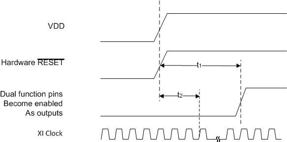 Figure 4-1 Power Up Timing
NOTE
It is important to choose pullup and-or pulldown resistors for each of the hardware configuration pins that provide fast RC time constants in order to latch in the proper value prior to the pin transitioning to an output driver.
4.9.2 Reset Timing
Table 4-2 Reset Timing
| PARAMETER | TEST CONDITIONS | MIN | TYP | MAX | UNIT | |
|---|---|---|---|---|---|---|
| t1 | RESET pulse width | XI Clock must be stable for minimum of 1µs during RESET pulse low time. | 1 | µs | ||
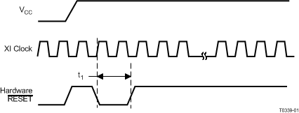 Figure 4-2 Reset Timing
4.9.3 MII Serial Management Timing
Table 4-3 MII Serial Management Timing
| PARAMETER | TEST CONDITIONS | MIN | TYP | MAX | UNIT | |
|---|---|---|---|---|---|---|
| t1 | MDC Frequency | 2.5 | 25 | MHz | ||
| t2 | MDC to MDIO (Output) Delay Time | 0 | 30 | ns | ||
| t3 | MDIO (Input) to MDC Hold Time | 10 | ns | |||
| t4 | MDIO (Input) to MDC Setup Time | 10 | ns | |||
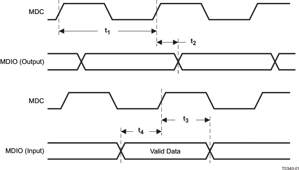 Figure 4-3 MII Serial Management Timing
4.9.4 100Mb/s MII Transmit Timing
Table 4-4 100Mb/s MII Transmit Timing
| PARAMETER | TEST CONDITIONS | MIN | TYP | MAX | UNIT | |
|---|---|---|---|---|---|---|
| t1 | TX_CLK High Time | 100Mbs Normal mode | 16 | 20 | 24 | ns |
| t2 | TX_CLK Low Time | |||||
| t3 | TXD[3:0], TX_EN Data Setup to TX_CLK | 100Mbs Normal mode | 10 | ns | ||
| t4 | TXD[3:0], TX_EN Data Hold from TX_CLK | 100Mbs Normal mode | 0 | ns | ||
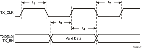 Figure 4-4 100Mb/s MII Transmit Timing
4.9.5 100Mb/s MII Receive Timing
Table 4-5 100Mb/s MII Receive Timing
| PARAMETER(1) | TEST CONDITIONS | MIN | TYP | MAX | UNIT | |
|---|---|---|---|---|---|---|
| t1 | RX_CLK High Time | 100Mbs Normal mode | 16 | 20 | 24 | ns |
| t2 | RX_CLK Low Time | |||||
| t3 | RX_CLK to RXD[3:0], RX_DV, RX_ER Delay | 100Mbs Normal mode | 10 | 30 | ns | |
 Figure 4-5 100Mb/s MII Receive Timing
4.9.6 100Base-TX Transmit Packet Latency Timing
Table 4-6 100Base-TX Transmit Packet Latency Timing
| PARAMETER | TEST CONDITIONS | MIN | TYP | MAX | UNIT | |
|---|---|---|---|---|---|---|
| t1 | TX_CLK to PMD Output Pair Latency | 100Mbs Normal mode(1) | 4.8 | bits(2) | ||
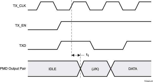 Figure 4-6 100Base-TX Transmit Packet Latency Timing
4.9.7 100Base-TX Transmit Packet Deassertion Timing
Table 4-7 100Base-TX Transmit Packet Deassertion Timing
| PARAMETER | TEST CONDITIONS | MIN | TYP | MAX | UNIT | |
|---|---|---|---|---|---|---|
| t1 | TX_CLK to PMD Output Pair deassertion | 100Mbs Normal mode | 4.6 | bits | ||
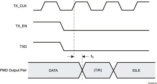 Figure 4-7 100Base-TX Transmit Packet Deassertion Timing
4.9.8 100Base-TX Transmit Timing (tR/F and Jitter)
Table 4-8 100Base-TX Transmit Timing (tR/F and Jitter)
| PARAMETER | TEST CONDITIONS | MIN | TYP | MAX | UNIT | |
|---|---|---|---|---|---|---|
| t1 | 100Mbs PMD Output Pair tR and tF (1) | 3 | 4 | 5 | ns | |
| 100Mbs tR and tF Mismatch(2) | 500 | ps | ||||
| t2 | 100Mbs PMD Output Pair Transmit Jitter | 1.4 | ns | |||
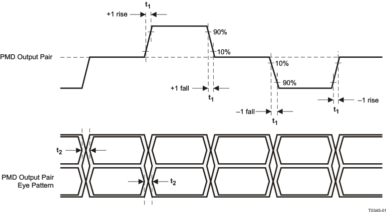 Figure 4-8 100Base-TX Transmit Timing (tR/F and Jitter)
4.9.9 100Base-TX Receive Packet Latency Timing
Table 4-9 100Base-TX Receive Packet Latency Timing
| PARAMETER | TEST CONDITIONS(3) | MIN | TYP | MAX | UNIT(2) | |
|---|---|---|---|---|---|---|
| t1 | Carrier Sense ON Delay(1) | 100Mbs normal mode | 14 | bits | ||
| t2 | Receive Data Latency | 100Mbs normal mode | 19 | |||
| t2 | Receive Data Latency(4) | 100Mbs normal mode with fast RXDV detection ON | 15 | |||
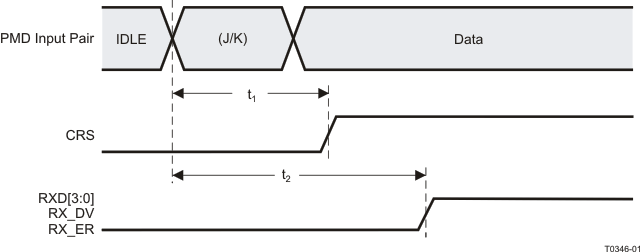 Figure 4-9 100Base-TX Receive Packet Latency Timing
4.9.10 100Base-TX Receive Packet Deassertion Timing
Table 4-10 100Base-TX Receive Packet Deassertion Timing
| PARAMETER | TEST CONDITIONS | MIN | TYP | MAX | UNIT | |
|---|---|---|---|---|---|---|
| t1 | Carrier Sense OFF Delay(1) | 100Mbs Normal mode | 19 | bits(2) | ||
 Figure 4-10 100Base-TX Receive Packet Deassertion Timing
4.9.11 10Mbs MII Transmit Timing
Table 4-11 10Mbs MII Transmit Timing
| PARAMETER | TEST CONDITIONS | MIN | TYP | MAX | UNIT | |
|---|---|---|---|---|---|---|
| t1 | TX_CLK Low Time | 10Mbs MII mode | 190 | 200 | 210 | ns |
| t2 | TX_CLK High Time | |||||
| t3 | TXD[3:0], TX_EN Data Setup to TX_CLK ↑ | 10Mbs MII mode | 25 | ns | ||
| t4 | TXD[3:0], TX_EN Data Hold from TX_CLK ↑ | 10Mbs MII mode | 0 | ns | ||
An attached Mac should drive the transmit signals using the positive edge of TX_CLK. As shown in Figure 4-11, the MII signals are sampled on the falling edge of TX_CLK.
 Figure 4-11 10Mbs MII Transmit Timing
4.9.12 10Mb/s MII Receive Timing
Table 4-12 10Mb/s MII Receive Timing
| PARAMETER(1) | TEST CONDITIONS | MIN | TYP | MAX | UNIT | |
|---|---|---|---|---|---|---|
| t1 | RX_CLK High Time | 160 | 200 | 240 | ns | |
| t2 | RX_CLK Low Time | |||||
| t3 | RX_CLK rising edge delay from RXD[3:0], RX_DV Valid | 10Mbs MII mode | 100 | ns | ||
| t4 | RX_CLK to RXD[3:0], RX_DV Delay | 10Mbs MII mode | 100 | ns | ||
 Figure 4-12 10Mb/s MII Receive Timing
4.9.13 10Base-T Transmit Timing (Start of Packet)
Table 4-13 10Base-T Transmit Timing (Start of Packet)
| PARAMETER | TEST CONDITIONS | MIN | TYP | MAX | UNIT(1) | |
|---|---|---|---|---|---|---|
| t1 | Transmit Output Delay from the Falling Edge of TX_CLK | 10Mbs MII mode | 5.8 | bits | ||
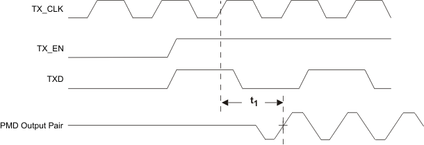 Figure 4-13 10Base-T Transmit Timing (Start of Packet)
4.9.14 10Base-T Transmit Timing (End of Packet)
Table 4-14 10Base-T Transmit Timing (End of Packet)
| PARAMETER | TEST CONDITIONS | MIN | TYP | MAX | UNIT | |
|---|---|---|---|---|---|---|
| t1 | End of Packet High Time (with ‘0’ ending bit) | 250 | 310 | ns | ||
| t2 | End of Packet High Time (with ‘1’ ending bit) | 250 | 310 | ns | ||
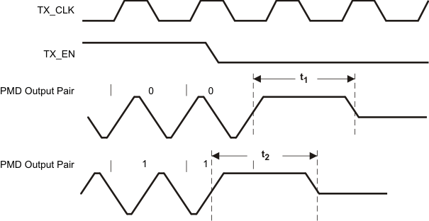 Figure 4-14 10Base-T Transmit Timing (End of Packet)
4.9.15 10Base-T Receive Timing (Start of Packet)
Table 4-15 10Base-T Receive Timing (Start of Packet)
| PARAMETER | TEST CONDITIONS | MIN | TYP | MAX | UNIT | |
|---|---|---|---|---|---|---|
| t1 | Carrier Sense Turn On Delay (PMD Input Pair to CRS) | 550 | 1000 | ns | ||
| t2 | RX_DV Latency(1) | 14 | bits | |||
| t3 | Receive Data Latency | Measurement shown from SFD | 14 | bits | ||
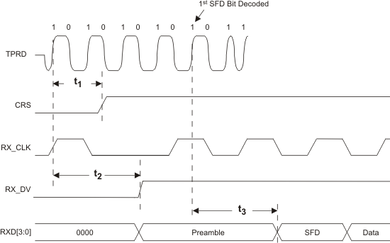 Figure 4-15 10Base-T Receive Timing (Start of Packet)
4.9.16 10Base-T Receive Timing (End of Packet)
Table 4-16 10Base-T Receive Timing (End of Packet)
| PARAMETER | TEST CONDITIONS | MIN | TYP | MAX | UNIT | |
|---|---|---|---|---|---|---|
| t1 | Carrier Sense Turn Off Delay | 1.8 | μs | |||
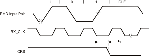 Figure 4-16 10Base-T Receive Timing (End of Packet)
4.9.17 10Mb/s Jabber Timing
Table 4-17 10Mb/s Jabber Timing
| PARAMETER | TEST CONDITIONS | MIN | TYP | MAX | UNIT | |
|---|---|---|---|---|---|---|
| t1 | Jabber Activation Time | 10 Mb/s MII mode | 100 | ms | ||
| t2 | Jabber Deactivation Time | 500 | ||||
 Figure 4-17 10Mb/s Jabber Timing
4.9.18 10Base-T Normal Link Pulse Timing
Table 4-18 10Base-T Normal Link Pulse Timing
| PARAMETER(1) | TEST CONDITIONS | MIN | TYP | MAX | UNIT | |
|---|---|---|---|---|---|---|
| t1 | Pulse Period | 10 Mb/s MII mode | 16 | ms | ||
| t2 | Pulse Width | 100 | ns | |||
 Figure 4-18 10Base-T Normal Link Pulse Timing
4.9.19 Auto-Negotiation Fast Link Pulse (FLP) Timing
Table 4-19 Auto-Negotiation Fast Link Pulse (FLP) Timing
| PARAMETER | TEST CONDITIONS | MIN | TYP | MAX | UNIT | |
|---|---|---|---|---|---|---|
| t1 | Clock Pulse to Clock Pulse Period | 125 | μs | |||
| t2 | Clock Pulse to Data Pulse Period | Data = 1 | 62 | μs | ||
| t3 | Clock, Data Pulse Width | 114 | ns | |||
| t4 | FLP Burst to FLP Burst Period | 16 | ms | |||
| t5 | Burst Width | 2 | ms | |||
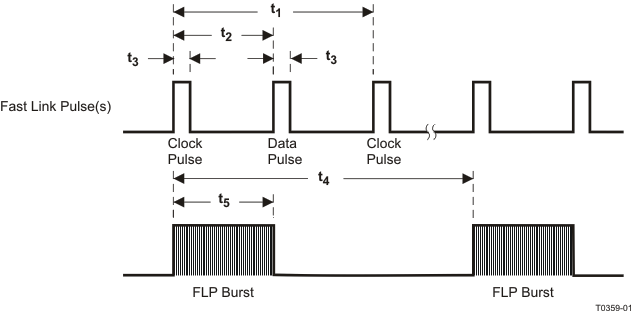 Figure 4-19 Auto-Negotiation Fast Link Pulse (FLP) Timing
4.9.20 100Base-TX Signal Detect Timing
Table 4-20 100Base-TX Signal Detect Timing
| PARAMETER | TEST CONDITIONS | MIN | TYP | MAX | UNIT | |
|---|---|---|---|---|---|---|
| t1 | SD Internal Turn-on Time | 100 | μs | |||
| t2 | Internal Turn-off Time | 200 | μs | |||

NOTE:
The signal amplitude on PMD Input Pair must be TP-PMD compliant.4.9.21 100Mbs Loopback Timing
Table 4-21 100Mbs Loopback Timing
| PARAMETER | TEST CONDITIONS | MIN | TYP | MAX | UNIT | |
|---|---|---|---|---|---|---|
| t1 | TX_EN to RX_DV Loopback | 100Mbs external loopback | 241 | 242 | 243 | ns |
| 100Mbs external loopback – fast RX_DV mode | 201 | 202 | 203 | |||
| 100Mbs analog loopback | 232 | 233 | 234 | |||
| 100Mbs PCS Input loop back | 120 | 121 | 122 | |||
| 100Mbs MII loop back | 8 | 9 | 10 | |||
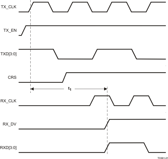
4.9.22 10Mbs Internal Loopback Timing
Table 4-22 10Mbs Internal Loopback Timing
| PARAMETER | TEST CONDITIONS | MIN | TYP | MAX | UNIT | |
|---|---|---|---|---|---|---|
| t1 | TX_EN to RX_DV Loopback | 10Mbs internal loopback mode | 1.7 | μs | ||
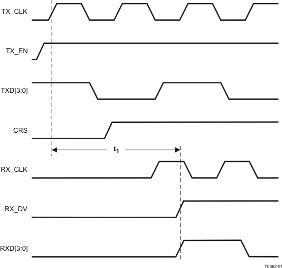
4.9.23 RMII Transmit Timing
Table 4-23 RMII Transmit Timing
| PARAMETER | TEST CONDITIONS | MIN | TYP | MAX | UNIT | |
|---|---|---|---|---|---|---|
| t1 | XI Clock Period | 50MHz Reference Clock | 20 | ns | ||
| t2 | TXD[1:0] and TX_EN data setup to X1 rising | 1.4 | ||||
| t3 | TXD[1:0] and TX_EN data hold to X1 rising | VDD_IO = 3.3V | 2.0 | |||
| VDD_IO = 2.5V | 4.9 | |||||
| t4 | XI Clock to PMD Output Pair Latency | 12 | bits | |||
 Figure 4-23 RMII Transmit Timing
4.9.24 RMII Receive Timing
Table 4-24 RMII Receive Timing
| PARAMETER | TEST CONDITIONS | MIN | TYP | MAX | UNIT | |
|---|---|---|---|---|---|---|
| t1 | XI Clock Period | 50MHz Reference Clock | 20 | ns | ||
| t2 | RXD[1:0], CRS_DV, RX_DV and RX_ER output delay from XI rising | 4 | 10.8 | 14 | ||
| t3 | CRS ON delay | From JK symbol on PMD Receive Pair to initial assertion of CRS_DV | 17.6 | bits | ||
| t4 | CRS OFF delay | From TR symbol on PMD Receive Pair to initial assertion of CRS_DV | 26.2 | |||
| t5 | RXD[1:0] and RX_ER latency | From symbol on Receive Pair. * Elasticity buffer set to default value (01) | 29.7 | |||
| t6 | RX_CLK Clock Period | 50MHz “Recovered clock” while working in “RMII receive clock” mode | 20 | ns | ||
| t7 | RXD[1:0], CRS_DV, RX_DV and RX_ER output delay from RX_CLK rising | While working in “RMII receive clock” mode | 3.8 | |||
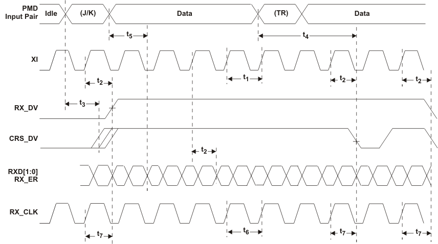 Figure 4-24 RMII Receive Timing
NOTE
- Per the RMII Specification, output delays assume a 25pF load.
- CRS_DV is asserted asynchronously in order to minimize latency of control signals through the PHY. CRS_DV may toggle synchronously at the end of the packet to indicate CRS de-assertion.
- RX_DV is synchronous to XI. While not part of the RMII specification, this signal is provided to simplify recovery of receive data.
- “RMII receive clock” mode is not part of the RMII specification that allows synchronization of the MAC-PHY RX interface in RMII mode. Setting register 0x000A bit [0] is required to activate this mode.
4.9.25 Isolation Timing
Table 4-25 Isolation Timing
| PARAMETER | TEST CONDITIONS | MIN | TYP | MAX | UNIT | |
|---|---|---|---|---|---|---|
| t1 | From Deassertion of S/W or H/W Reset to transition from Isolate to Normal mode | 71 | ns | |||
 Figure 4-25 Isolation Timing