-
TPS6206x 3-MHz, 1.6-A, Step Down Converter in 2-mm × 2-mm WSON Package
- 1 Features
- 2 Applications
- 3 Description
- 4 Revision History
- 5 Device Comparison Table
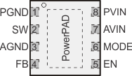
- 6 Pin Configuration and Functions
- 7 Specifications
- 8 Detailed Description
- 9 Application and Implementation
- 10Power Supply Recommendations
- 11Layout
- 12Device and Documentation Support
- 13Mechanical, Packaging, and Orderable Information
- IMPORTANT NOTICE
パッケージ・オプション
メカニカル・データ(パッケージ|ピン)
- DSG|8
サーマルパッド・メカニカル・データ
- DSG|8
発注情報
TPS6206x 3-MHz, 1.6-A, Step Down Converter in 2-mm × 2-mm WSON Package
1 Features
- 3-MHz Switching Frequency
- VIN Range from 2.7 V to 6 V
- 1.6-A Output Current
- Up to 97% Efficiency
- Power Save Mode and 3-MHz Fixed PWM Mode
- Output Voltage Accuracy in PWM Mode ±1.5%
- Output Discharge Function
- Typical 18-µA Quiescent Current
- 100% Duty Cycle for Lowest Dropout
- Voltage Positioning
- Clock Dithering
- Supports Maximum 1-mm Height Solutions
- Available in a 2 mm × 2 mm × 0.75 mm WSON
2 Applications
- Point of Load (POL)
- Notebooks, Pocket PCs
- Portable Media Players
- DSP Supplies
3 Description
The TPS6206x is a family of highly efficient synchronous step-down DC-DC converters. They provide up to 1.6-A output current.
With an input voltage range of 2.7 V to 6 V, the device is a perfect fit for power conversion from a single Li-Ion battery as well from 5-V or 3.3-V system supply rails. The TPS6206x operates at 3-MHz fixed frequency and enters power save mode operation at light load currents to maintain high efficiency over the entire load current range. The power save mode is optimized for low output voltage ripple. For low noise applications, the device can be forced into fixed frequency PWM mode by pulling the MODE pin high.
In the shutdown mode, the current consumption is reduced to less than 1 µA and an internal circuit discharges the output capacitor.
TPS6206x family is optimized for operation with a tiny 1-µH inductor and a small 10-µF output capacitor to achieve smallest solution size and high regulation performance.
The TPS6206x operates over a free air temperature of –40°C to 85°C. The device is available in a small 2-mm × 2-mm × 0.75-mm 8-pin WSON PowerPAD™ integrated circuit package.
Device Information(1)
| PART NUMBER | PACKAGE | BODY SIZE (NOM) |
|---|---|---|
| TPS62060 TPS62061 TPS62063 |
WSON (8) | 2.00 mm × 2.00 mm |
- For all available packages, see the orderable addendum at the end of the data sheet.
Typical Application Schematic

Efficiency vs Load Current

4 Revision History
Changes from A Revision (January 2011) to B Revision
- Added Pin Configuration and Functions section, ESD Ratings table, Feature Description section, Device Functional Modes, Application and Implementation section, Power Supply Recommendations section, Layout section, Device and Documentation Support section, and Mechanical, Packaging, and Orderable Information section Go
5 Device Comparison Table(2)
| PART NUMBER | OUTPUT VOLTAGE(1) | FUNCTION | MAXIMUM OUTPUT CURRENT | PACKAGE DESIGNATOR | PACKAGE MARKING | |
|---|---|---|---|---|---|---|
| MODE | Power Good (PG) | |||||
| TPS62060 | Adjustable | Selectable | No | 1.6 A | DSG | CGY |
| TPS62061 | 1.8 V fix | Selectable | No | 1.6 A | CGX | |
| TPS62063 | 3.3 V fix | Selectable | No | 1.6 A | QXD | |
| TPS6206x(1) | Adjustable | no | yes | 1.6 A | — | |
6 Pin Configuration and Functions

Pin Functions
| PIN | TYPE | DESCRIPTION | |
|---|---|---|---|
| NAME | NO. | ||
| AGND | 3 | I | Analog GND supply pin for the control circuit. |
| AVIN | 7 | I | Analog VIN power supply for the control circuit. Must be connected to PVIN and input capacitor. |
| EN | 5 | I | This is the enable pin of the device. Pulling this pin to low forces the device into shutdown mode. Pulling this pin to high enables the device. This pin must be terminated |
| FB | 4 | I | Feedback pin for the internal regulation loop. Connect the external resistor divider to this pin. In case of fixed output voltage option, connect this pin directly to the output capacitor |
| MODE | 6 | I | When MODE pin = High forces the device to operate in fixed frequency PWM mode. When MODE pin = Low enables the power save mode with automatic transition from PFM mode to fixed frequency PWM mode. |
| PGND | 1 | PWR | GND supply pin for the output stage. |
| PVIN | 8 | PWR | VIN power supply pin for the output stage. |
| SW | 2 | O | This is the switch pin and is connected to the internal MOSFET switches. Connect the external inductor between this terminal and the output capacitor. |
| PowerPAD | — | For good thermal performance, this PAD must be soldered to the land pattern on the PCB. This PAD should be used as device GND. | |