-
TPS62480 2.4-V to 5.5-V, 6-A, 2-Phase Step-Down Converter
- 1 Features
- 2 Applications
- 3 Description
- 4 Revision History
- 5 Pin Configuration and Functions
- 6 Specifications
- 7 Detailed Description
- 8 Application and Implementation
- 9 Power Supply Recommendations
- 10Layout
- 11Device and Documentation Support
- 12Mechanical, Packaging, and Orderable Information
- IMPORTANT NOTICE
TPS62480 2.4-V to 5.5-V, 6-A, 2-Phase Step-Down Converter
1 Features
- Dual Phase Current Mode Topology
- Input Voltage Range 2.4 to 5.5 V
- Output Voltage Range 0.6 to 5.5 V
- Output Current of 6 A
- Typical Quiescent Current of 23 µA
- Feedback Voltage Accuracy of ±1% (PWM Mode)
- Output Voltage Select
- Phase Shifted Operation
- Automatic Power Save Modes
- Forced PWM Mode
- Adjustable Soft Start
- Power Good / Thermal Good Outputs
- Undervoltage Lockout
- Overcurrent and Short-Circuit Protection
- Overtemperature Protection
- 3 × 2.5 mm HotRod™ Package
2 Applications
- Low Profile Point-of-Load Supply
- Solid State Drives
- Ultra Portable/Tablet/Embedded PC
- Optical Modules, CMOS Cameras
- Wireless Modules, Network Cards
3 Description
The TPS62480 is a synchronous 2-phase step-down DC-DC converter for low profile point-of-load power supplies. The input voltage range of 2.4 to 5.5 V enables operation from typical 3.3-V or 5-V interface supplies as well as from backup circuits dropping down as low as 2.4 V. The output current is up to 6 A continuously provided by two phases of 3 A each, allowing the use of low-profile external components. Both the rails are running out of phase, reducing pulse current noise significantly.
The TPS62480 provides an automatically entered power save mode to maintain high efficiency down to very light loads. This incorporates an automatic phase adding and shedding feature using both or only one phase according to the actual load.
The device features a Power Good signal and an adjustable soft start. Also, the device features a Thermal Good signal to detect excessive internal temperature. The output voltage can be changed to a preselected value by VSEL pin. TPS62480 is able to operate in 100% duty cycle mode.
The TPS62480 is packaged in a small 3 × 2.5 mm HotRod™ package (RNC).
Device Information(1)
| PART NUMBER | PACKAGE | BODY SIZE (NOM) |
|---|---|---|
| TPS62480 | VQFN (16) | 3.00 × 2.50 mm |
- For all available packages, see the orderable addendum at the end of the data sheet.
space
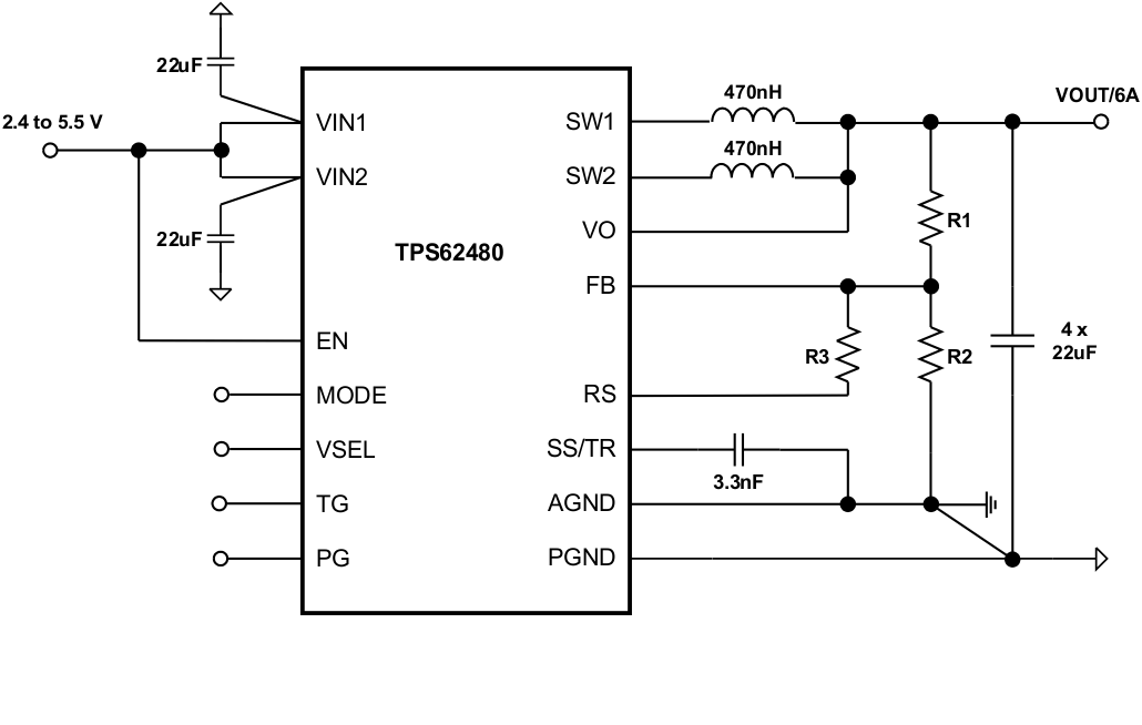
Typical Application Schematic |
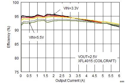
Efficiency vs Output Current |
|
 |
space |
|
 |
||
4 Revision History
Changes from * Revision (February 2016) to A Revision
- Changed RCN Package To: RNC Package in Pin Configuration and FunctionsGo
- Changed RCN 16 PINS To: RNC 16 PINS in the Thermal Information tableGo
- Changed the Test Conditions for ISD Shutdown Current From: EN = Low (≤ 0.4 V) To: EN = Low (≤ 0.3 V) in the Electrical CharacteristicsGo
- Changed the VOUT Feedback Voltage Accuracy, MAX value From: 25% To: 2.5% in the Electrical CharacteristicsGo
- Changed TPS62480RCN To: TPS62480RNC in Table 1Go
5 Pin Configuration and Functions

space
space
Pin Functions
| PIN | I/O | DESCRIPTION | |
|---|---|---|---|
| NAME | NO. | ||
| PGND1 | 1 | Power Ground Phase 1 (master) | |
| SW1 | 2 | Switch Node Phase 1 (master) , connected to the internal MOSFET switches | |
| VIN1 | 3 | Supply voltage Phase 1 (master) | |
| EN | 4 | I | Enable input (High=Enabled, Low = Disabled) |
| PG | 5 | O | Power Good (open drain, requires pull-up resistor) |
| VSEL | 6 | I | Output Voltage Select (High = VOUT2, Low=VOUT1) , VOUT1 < VOUT2 |
| TG | 7 | O | Thermal Good (open drain, requires pull-up resistor) |
| MODE | 8 | I | Operating mode selection (Low=Automatic PWM/PSM, High = Forced PWM) |
| VIN2 | 9 | Supply voltage Phase 2 | |
| SW2 | 10 | Switch node Phase 2, connected to the internal MOSFET switches | |
| PGND2 | 11 | Power Ground Phase 2 | |
| SS/TR | 12 | O | Soft-Start / Tracking. An external capacitor connected to this pin sets the output voltage rise time. |
| AGND | 13 | Analog Ground | |
| FB | 14 | Output voltage feedback for the adjustable version. Connect resistive voltage divider to this pin. | |
| RS | 15 | Resistor Select. Connect resistor that sets the level for the second output voltage here (activated by VSEL= High) | |
| VO | 16 | VOUT detection (connect to VOUT, output discharge is internally connected to this pin) | |
6 Specifications
6.1 Absolute Maximum Ratings
over operating free-air temperature range (unless otherwise noted) (1)| MIN | MAX | UNIT | ||
|---|---|---|---|---|
| Pin Voltage Range(2) | VIN | -0.3 | 6 | V |
| SW1, SW2 | -0.3 | VIN+0.3 | V | |
| EN, VSEL, MODE, SS/TR, PG, TG | -0.3 | 6 | V | |
| FB, RS | -0.3 | 3 | V | |
| Power Good / Thermal Good Sink Current | PG, TG | 10 | mA | |
| Operating Junction Temperature Range, TJ | -40 | 150 | °C | |
| Storage Temperature Range, Tstg | -65 | 150 | °C | |
6.2 ESD Ratings
| VALUE | UNIT | |||
|---|---|---|---|---|
| V(ESD) | Electrostatic discharge | Human body model (HBM), per ANSI/ESDA/JEDEC JS-001, all pins(1) | ±1000 | V |
| Charged device model (CDM), per JEDEC specification JESD22-C101, all pins(2) | ±500 | |||
6.3 Recommended Operating Conditions
over operating junction temperature range (unless otherwise noted)| MIN | TYP | MAX | UNIT | ||
|---|---|---|---|---|---|
| Supply Voltage Range, VIN | 2.4 | 5.5 | V | ||
| Output Voltage Range, VOUT | 0.6 | 5.5 | V | ||
| Maximum Output Current, IOUT | 6 | A | |||
| Operating junction temperature, TJ | –40 | 125 | °C | ||
6.4 Thermal Information
| THERMAL METRIC(1) | TPS62480 | UNIT | ||
|---|---|---|---|---|
| RNC 16 PINS | ||||
| JEDEC with thermal vias(2) | JEDEC standard | |||
| RθJA | Junction-to-ambient thermal resistance | 26.4 | 56.4 | °C/W |
| RθJC(top) | Junction-to-case (top) thermal resistance | 32.2 | 32.2 | °C/W |
| RθJB | Junction-to-board thermal resistance | 10.2 | 26.5 | °C/W |
| ψJT | Junction-to-top characterization parameter | 0.9 | 1.3 | °C/W |
| ψJB | Junction-to-board characterization parameter | 10.2 | 26.5 | °C/W |
| RθJC(bot) | Junction-to-case (bottom) thermal resistance | - | - | °C/W |
6.5 Electrical Characteristics
over operating junction temperature range (TJ = –40°C to 125°C) and VIN = 2.4 V to 5.5 V. Typical values at VIN = 3.6 V and TJ = 25°C (unless otherwise noted).| PARAMETER | TEST CONDITIONS | MIN | TYP | MAX | UNIT | ||
|---|---|---|---|---|---|---|---|
| SUPPLY | |||||||
| VIN | Input Voltage Range | VIN rising | 2.6 | 5.5 | V | ||
| VIN falling | 2.4 | 5.5 | |||||
| IQ | Operating Quiescent Current | EN = High, VIN ≥ 3 V, IOUT = 0 mA, device not switching, TJ = -40°C to +85°C |
23 | 38 | µA | ||
| 100% Mode operation | 3.5 | 6.5 | mA | ||||
| ISD | Shutdown Current | EN = Low (≤ 0.3 V), TJ = -40°C to +85°C | 0.5 | 18.5 | µA | ||
| VUVLO | Undervoltage Lockout Threshold | Falling Input Voltage | 2.2 | 2.3 | 2.4 | V | |
| Hysteresis | 200 | mV | |||||
| TSD | Thermal Shutdown Temperature | PWM Mode, Rising Junction Temperature | 160 | °C | |||
| Thermal Shutdown Hysteresis | PWM Mode | 10 | |||||
| CONTROL (EN, VSEL, MODE, SS/TR, PG, TG) | |||||||
| VH | Input Threshold Voltage (EN, VSEL, MODE) | to ensure High Level | 1.2 | V | |||
| VL | Input Threshold Voltage (EN, VSEL, MODE) | to ensure Low Level | 0.4 | ||||
| ILKG(EN) | Input Leakage Current (EN) | EN = VIN or GND | 10 | 200 | nA | ||
| ILKG(MODE) | Input Leakage Current (MODE, VSEL) | 10 | 200 | nA | |||
| ISS/TR | SS/TR pin source current | 4.7 | 5.25 | 5.8 | µA | ||
| VTH(TG) | Thermal Good Threshold Temperature | PWM Mode | 120 | °C | |||
| Thermal Good Hysteresis | PWM Mode | 10 | |||||
| VTH(PG) | Power Good Threshold Voltage | Rising (%VOUT) | 93% | 96% | 99% | ||
| Falling (%VOUT) | 89% | 92% | 95% | ||||
| VL(PG) | Output Low Threshold (PG, TG) | IPG = -2 mA | 0.4 | V | |||
| ILKG(PG) | Input Leakage Current (PG) | 2 | 700 | nA | |||
| ILKG(TG) | Input Leakage Current (TG) | 2 | 100 | nA | |||
| tSS | Internal Soft-Start Time | SS/TR = VIN or floating | 80 | µs | |||
| tDELAY | Time from EN rising until start switching | 100 | 200 | 400 | µs | ||
| POWER SWITCH | |||||||
| RDS(ON) | High-Side MOSFET ON-Resistance |
VIN ≥ 3 V | Phase1 | 36 | 98 | mΩ | |
| Phase2 | |||||||
| Low-Side MOSFET ON-Resistance |
Phase1 | 29 | 72 | mΩ | |||
| Phase2 | |||||||
| ILIM | High-Side MOSFET Current Limit |
per phase | 4.3 | 5.0 | 5.8 | A | |
| OUTPUT | |||||||
| VREF | Internal Reference Voltage | 0.6 | V | ||||
| ILKG(FB) | Input Leakage Current (FB) | EN = High | VFB = 0.6 V | 1 | 65 | nA | |
| ILKG(RS) | Input Leakage Current (RS) | VSEL = Low, VRS = 0.6 V | 1 | 65 | nA | ||
| RRS | Internal resistance (RS to GND) | VSEL = High, IRS = 1 mA | 10 | 50 | Ω | ||
| VOUT | Output Voltage Range | VIN ≥ VOUT | 0.6 | 5.5 | V | ||
| VOUT | Feedback Voltage Accuracy | PWM Mode, VIN ≥ VOUT + 1 V |
TJ = –20°C to 85°C | -1% | 1% | ||
| TJ = –40°C to 125°C | -1.4% | 1.3% | |||||
| VOUT | Feedback Voltage Accuracy | Power Save Mode, L = 0.47 µH, COUT = 4 x 22 µF(1) |
-1.4% | 2.5% | |||
| Output Discharge Current(2) | EN = Low, VOUT = 2.5 V | 120 | mA | ||||
| Load Regulation | VOUT = 1.8 V, PWM mode operation | 0.02 | %/A | ||||
| Line Regulation | 2.6 V ≤ VIN ≤ 5.5 V, VOUT = 1.8 V, IOUT = 6 A, PWM mode operation | 0.02 | %/V | ||||
6.6 Typical Characteristics


