SLVSBC9C March 2012 – February 2016 TPS65177 , TPS65177A
PRODUCTION DATA.
- 1 Features
- 2 Applications
- 3 Description
- 4 Revision History
- 5 Pin Configuration and Functions
- 6 Specifications
-
7 Detailed Description
- 7.1 Overview
- 7.2 Functional Block Diagram
- 7.3 Feature Description
- 7.4
Device Functional Modes
- 7.4.1 Boost Converter (V(AVDD))
- 7.4.2 Buck 1 Converter (V(IO))
- 7.4.3 BUCK 2 CONVERTER (V(CORE))
- 7.4.4 Buck 3 Converter (V(HAVDD))
- 7.4.5 Positive Charge Pump Controller (V(GH)) with Temperature Compensation
- 7.4.6 Negative Charge Pump Controller (V(GL))
- 7.5 Gate Pulse Modulation (V(GHM))
- 7.6
Programming
- 7.6.1 I2C Serial Interface Description
- 7.6.2 Memory Description
- 7.6.3 Read / Write Description
- 7.6.4 Write Operation
- 7.6.5 READ OPERATION
- 7.6.6 Write Single Data to DAC:
- 7.6.7 Write Multiple Data to DAC (Auto Increment Address):
- 7.6.8 Write all DAC Data to EEPROM:
- 7.6.9 Read Single Data From DAC / EEPROM:
- 7.6.10 Read Multiple Data fFom DAC / EEPROM (Auto Increment Address):
- 7.7
Register Map
- 7.7.1
Registers and DAC Settings
- 7.7.1.1 Channel Register (with factory value) - 00h (00h)
- 7.7.1.2 Boost Output Voltage V(AVDD) Register (with factory value) - 01h (0Fh)
- 7.7.1.3 Boost HVS Offset Voltage Register (with factory value) - 02h (05h)
- 7.7.1.4 Boost Current Limit Negative Offset Current Register (with factory value) - 03h (00h)
- 7.7.1.5 Boost Soft-start Time Register (with factory value) - 04h (00h)
- 7.7.1.6 Buck 1 Output Voltage V(IO) Register (with factory value) - 05h (03h):
- 7.7.1.7 Buck 2 Output Voltage V(CORE) Register (with factory value) - 06h (02h)
- 7.7.1.8 Buck 3 Output Voltage V(HAVDD) Register (with factory value) - 07h (1Bh)
- 7.7.1.9 Pos. Charge Pump Low Output Voltage V(GH_L) Register (with factory value) - 08h (08h):
- 7.7.1.10 Positive Charge Pump Low Output Voltage V(GH_L) to V(GH_H) Positive Offset Voltage V(GH_OFS) Register (with factory value) - 09h (04h):
- 7.7.1.11 Gate Pulse Modulation Limit Voltage Register (with factory value) - 0Ah (00h)
- 7.7.1.12 Negative Charge Pump Output Voltage V(GL) Register (with factory value) - 0Bh (04h)
- 7.7.1.13 Buck 3 HVS Offset Voltage Register (with factory value) - 0Ch (00h):
- 7.7.1.14 Memory Write Remain Time Register (with factory value) - FEh (0Fh):
- 7.7.1
Registers and DAC Settings
- 8 Application and Implementation
- 9 Power Supply Recommendations
- 10Layout
- 11Device and Documentation Support
- 12Mechanical, Packaging, and Orderable Information
1 Features
- Enable / Disable
- TPS65177: AVI power cycle
- TPS65177A: VI power cycle or EN-pin
- 8.6-V to 14.7-V Input Voltage Range
- Non-Synchronous Boost Converter (V(AVDD))
- Integrated Isolation Switch
- 13.5-V to 19.8-V Output Voltage (I2C)
- 15-V Default Output Voltage
- 4.25-A Switch Current Limit (I2C)
- High Voltage Stress Mode (I2C)
- Synchronous Buck Converter (V(HAVDD))
- 4.8-V to 11.1-V Output Voltage (I2C)
- 7.5-V Default Output Voltage
- 1.7-A Switch Current Limit
- High Voltage Stress Mode (I2C)
- Non-Synchronous Buck Converter (V(IO))
- 2.2-V to 3.7-V Output Voltage (I2C)
- 2.5-V Default Output Voltage
- 3-A Switch Current Limit
- Synchronous Buck Converter (V(CORE))
- 0.8-V to 3.3-V Output Voltage (I2C)
- 1-V Default Output Voltage
- 2.5-A Switch Current Limit
- Positive Charge-Pump Controller (V(GH))
- 20-V to 40-V Output Voltage (I2C)
- 28-V Default Output Voltage
- Temp. Compensation Offset 0-V to 15-V (I2C)
- 4-V Default Offset (28 V to 32 V)
- Negative Charge-Pump Controller (V(GL))
- –14.5-V to –5.5-V Output Voltage (I2C)
- –7.9-V Default Output Voltage
- Gate Pulse Modulation (GPM)
- Down to 0-V, 5-V, 10-V or 15-V (I2C)
- 0-V Default Discharge Voltage
- Temperature Compensation for V(GH)
- Thermal Shutdown
- I2C Compatible Interface
- EEPROM Memory
- 6-mm × 6-mm × 1-mm 40-Pin VQFN Package
2 Applications
- GIP (Gate-in-Panel) LCD TVs
- Non-GIP LCD TVs
3 Description
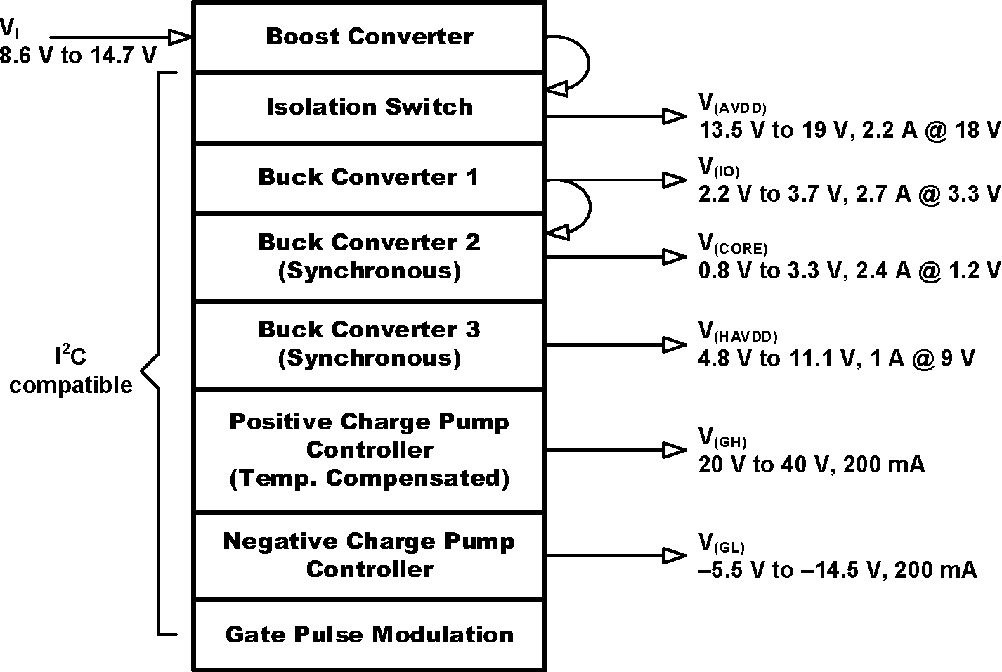
The TPS65177/A provides all supply rails needed by a GIP (Gate-in-Panel) or non-GIP TFT-LCD panel. All output voltages are I2C programmable.
V(IO) and V(CORE) for the T-CON, V(AVDD) and V(HAVDD) for the Source Driver and the Gamma Buffer, V(GH) and V(GL) for the Gate Driver or the Level Shifter. For use with non-GIP technology Gate Pulse Modulation (GPM) is implemented, for use with GIP technology the V(GH) rail can be temperature compensated. Furthermore a High Voltage Stress Mode (HVS) for V(AVDD) and V(HAVDD) and an integrated V(AVDD) Isolation Switch is implemented. V(CORE), V(HAVDD), V(GH), V(GL), GPM and the V(GH) temperature compensation can be enabled and disabled by I2C programming.
A single BOM (Bill of Materials) can cover several panel types and sizes whose desired output voltage levels can be programmed in production and stored in a non-volatile integrated memory.
Device Information(1)
| PART NUMBER | PACKAGE | BODY SIZE (NOM) |
|---|---|---|
| TPS65177 | VQFN (40 Pin) | 6.00 mm x 6.00 mm |
| TPS65177A | VQFN (40 Pin) | 6.00 mm x 6.00 mm |
- For all available packages, see the orderable addendum at the end of the data sheet.
Block Diagram

4 Revision History
Changes from B Revision (January 2016) to C Revision
- Added TPS65177A device and changed Features description, color of several graphics Go
Changes from A Revision (July 2012) to B Revision
- Added the ESD Ratings table, Features Description section, Device Functional Modes section, Application and Implementation section, Power Supply Recommendation section, Layout section, Device and Documentation Support section, and Mechanical, Packaging, and Orderable Information sections. Go
- Added text to the Power-Up section, " If the EN pin is not connected to VIN..."Go
Changes from * Revision (March 2012) to A Revision