SLVSAI3A September 2010 – May 2016
PRODUCTION DATA.
- 1 Features
- 2 Applications
- 3 Description
- 4 Revision History
- 5 Pin Configuration and Functions
- 6 Specifications
- 7 Detailed Description
- 8 Application and Implementation
- 9 Power Supply Recommendations
- 10Layout
- 11Device And Documentation Support
- 12Mechanical, Packaging, And Orderable Information
パッケージ・オプション
メカニカル・データ(パッケージ|ピン)
サーマルパッド・メカニカル・データ
発注情報
1 Features
- Qualified for Automotive Applications
- AEC-Q100 Qualified With the Following Results:
- Device Temperature Grade 1: –40°C to 125°C Ambient Operating Temperature Range
- Device HBM ESD Classification Level 2
- Device CDM ESD Classification Level C4B
- Stable With No Output Capacitor or Any Value or Type of Capacitor
- Input Voltage Range of 1.7 V to 5.5 V
- Ultra-Low Dropout Voltage: 75-mV Typical
- Excellent Load Transient Response—With Or Without Optional Output Capacitor
- New NMOS Topology Delivers Low Reverse Leakage Current
- Low Noise: 30-μVRMS Typical (10 Hz to 100 kHz)
- 0.5% Initial Accuracy
- 1% Overall Accuracy Over Line, Load, and Temperature
- Less Than 1-μA Maximum IQ in Shutdown Mode
- Thermal Shutdown and Specified Minimum and Maximum Current Limit Protection
- Available in Multiple Output Voltage Versions
- Fixed Outputs of 1.2 V to 3.3 V
- Adjustable Output from 1.2 V to 5.5 V
2 Applications
- Infotainment
- ADAS
- Automotive Clusters
- Body Control Modules
3 Description
The TPS736xx-Q1 family of low-dropout (LDO) linear voltage regulators uses a new topology: an NMOS pass element in a voltage-follower configuration. This topology is stable using output capacitors with low ESR, and even allows operation without a capacitor. It also provides high reverse blockage (low reverse current) and ground pin current that is nearly constant over all values of output current.
The TPS736xx-Q1 uses an advanced BiCMOS process to yield high precision while delivering very low dropout voltages and low ground pin current. Current consumption, when not enabled, is under 1 μA and ideal for portable applications. The extremely low output noise (30 μVRMS with 0.1-μF CNR) is ideal for powering VCOs. These devices are protected by thermal shutdown and foldback current limit.
Device Information(1)
| PART NUMBER | PACKAGE | BODY SIZE (NOM) |
|---|---|---|
| TPS73601-Q1, TPS73625-Q1, TPS73633-Q1 | SOT-23 (5) | 2.90 mm 1.60 mm |
- For all available packages, see the orderable addendum at the end of the data sheet.
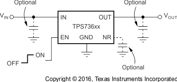
Typical Application
