SLVSCD1C December   2013  – November 2015 TPS92561

PRODUCTION DATA.  

  1. Features
  2. Applications
  3. Description
  4. Revision History
  5. Pin Configuration and Functions
  6. Specifications
    1. 6.1 Absolute Maximum Ratings
    2. 6.2 ESD Ratings
    3. 6.3 Recommended Operating Conditions
    4. 6.4 Thermal Information
    5. 6.5 Electrical Characteristics
    6. 6.6 Typical Characteristics
  7. Detailed Description
    1. 7.1 Overview
    2. 7.2 Functional Block Diagram
    3. 7.3 Feature Description
      1. 7.3.1 Basics of Operation
      2. 7.3.2 Sample Scope Capture
      3. 7.3.3 Output Current Control (ADJ, SEN)
      4. 7.3.4 Overcurrent Protection
      5. 7.3.5 Overvoltage Protection (OVP)
      6. 7.3.6 VCC Bias Supply and Start-Up
      7. 7.3.7 VCC and VP Connection
    4. 7.4 Device Functional Modes
  8. Application and Implementation
    1. 8.1 Application Information
      1. 8.1.1 Setting the Output Current
      2. 8.1.2 Selecting an Inductance
      3. 8.1.3 Important Design Consideration: Diode in Parallel With Sense Resistance
      4. 8.1.4 Gate Driver Operation
      5. 8.1.5 Output Bulk Capacitor
      6. 8.1.6 Phase Dimming
      7. 8.1.7 Example Circuits
    2. 8.2 Typical Applications
      1. 8.2.1 Offline Boost Schematic for Design Example
        1. 8.2.1.1 Design Requirements
        2. 8.2.1.2 Detailed Design Procedure
          1. 8.2.1.2.1 Set the LED Current
            1. 8.2.1.2.1.1 Calculate ADJ Pin Resistors
            2. 8.2.1.2.1.2 Calculate the Current Sense Resistor
            3. 8.2.1.2.1.3 Calculate the SEN Pin Series Resistance
          2. 8.2.1.2.2 Calculate OVP Pin Resistors
          3. 8.2.1.2.3 Calculate Inductor Value and Ripple Current
          4. 8.2.1.2.4 Calculate the Output Capacitor Value
      2. 8.2.2 11-W, 120-VAC Input, 225-V Output, Offline Boost Design Example
        1. 8.2.2.1 Design Requirements
        2. 8.2.2.2 Detailed Design Procedure
          1. 8.2.2.2.1 Set the LED Current
            1. 8.2.2.2.1.1 Calculate ADJ Pin Resistors
            2. 8.2.2.2.1.2 Calculate the Current Sense Resistor
            3. 8.2.2.2.1.3 Calculate the SEN Pin Series Resistance
          2. 8.2.2.2.2 Calculate OVP Pin Resistors
          3. 8.2.2.2.3 Calculate Inductor Value and Ripple Current
          4. 8.2.2.2.4 Calculate the Output Capacitor Value
        3. 8.2.2.3 Application Curve
  9. Power Supply Recommendations
  10. 10Layout
    1. 10.1 Layout Guidelines
    2. 10.2 Layout Example
  11. 11Device and Documentation Support
    1. 11.1 Documentation Support
      1. 11.1.1 Related Documentation
    2. 11.2 Community Resources
    3. 11.3 Trademarks
    4. 11.4 Electrostatic Discharge Caution
    5. 11.5 Glossary
  12. 12Mechanical, Packaging, and Orderable Information

パッケージ・オプション

メカニカル・データ(パッケージ|ピン)
サーマルパッド・メカニカル・データ
発注情報

1 Features

  • Simple Hysteretic Control
  • Compact Solution and Simple Bill Of Materials
  • Naturally Dimmable TRIAC and Reverse Phase Dimmers
  • Implements LED Drive Circuits Capable of High >90% Efficiency, >0.9 Power Factor, and <20% THD
  • Programmable Output Over-voltage Protection
  • Overtemperature Shutdown
  • VCC Undervoltage Lockout
  • 8-Pin VSSOP (MSOP) With Exposed Pad

2 Applications

  • Off-Line TRIAC Dimmable Applications
  • Off-Line Non-Dimmable Lamps
  • Lamps Requiring the Highest Efficiency and Lowest BOM Cost
  • Industrial and Commercial Solid State Lighting

3 Description

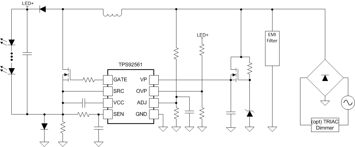
The TPS92561 device is a boost controller for LED lighting applications utilizing high-voltage, low-current LEDs. A boost converter approach to lighting applications allows the creation of the smallest volume converter possible and enables high efficiencies beyond 90%. The device incorporates a current sense comparator with a fixed offset enabling a simple hysteretic control scheme free of the loop compensation issues typically associated with a boost converter. The integrated OVP and VCC regulator further simplify the design procedure and reduce external component count.

Device Information(1)

PART NUMBER PACKAGE BODY SIZE (NOM)
TPS92561 HVSSOP (8) 3.00 mm × 3.00 mm
  1. For all available packages, see the orderable addendum at the end of the data sheet.

Typical Application Schematic
TPS92561 fbd_FAD_SLVSCD1.gif