SCES854A May 2014 – September 2017 TXS0102-Q1
PRODUCTION DATA.
- 1 Features
- 2 Applications
- 3 Description
- 4 Revision History
- 5 Pin Configuration and Functions
-
6 Specifications
- 6.1 Absolute Maximum Ratings
- 6.2 ESD Ratings
- 6.3 Recommended Operating Conditions
- 6.4 Thermal Information
- 6.5 Electrical Characteristics
- 6.6 Timing Requirements — VCCA = 1.8 V ± 0.15 V
- 6.7 Timing Requirements — VCCA = 2.5 V ± 0.2 V
- 6.8 Timing Requirements — VCCA = 3.3 V ± 0.3 V
- 6.9 Switching Characteristics — VCCA = 1.8 V ± 0.15 V
- 6.10 Switching Characteristics — VCCA = 2.5 V ± 0.2 V
- 6.11 Switching Characteristics — VCCA = 3.3 V ± 0.3 V
- 6.12 Typical Characteristics
- 7 Parameter Measurement Information
- 8 Detailed Description
- 9 Application and Implementation
- 10Power Supply Recommendations
- 11Layout
- 12Device and Documentation Support
- 13Mechanical, Packaging, and Orderable Information
1 Features
- Qualified for Automotive Applications
- AEC-Q100 Qualified With the Following Results:
- Device Temperature Grade 1: –40°C to +125°C Ambient Operating Temperature Range
- Device HBM ESD Classification Level 2
- Device CDM ESD Classification Level C5
- ESD Protection per JESD 22
- A Port
- 2500-V Human-Body Model (A114-B)
- 750-V Charged-Device Model (C101)
- B Port
- 8-kV Human-Body Model (A114-B)
- 750-V Charged-Device Model (C101)
- A Port
- No Direction-Control Signal Required
- Maximum Data Rates
- 24 Mbps Maximum (Push Pull)
- 2 Mbps (Open Drain)
- Available in the Texas Instruments NanoFree™ Package
- 1.65 V to 3.6 V on A port and 2.3 V to 5.5 V on B port (VCCA ≤ VCCB)
- No Power-Supply Sequencing Required—VCCA or VCCB can be Ramped First
2 Applications
- Automotive Infotainment
- Advance Driver-Assistance Systems (ADAS)
- Isolates and Level-Translates Between Main Processor and Peripheral Modules
- I2C or 1-Wire Voltage-Level Translation
3 Description
The TXS0102-Q1 device connects an incompatible logic communication from chip-to-chip due to voltage mismatch. This auto-direction translator can be conveniently used to bridge the gap without the need of direction control from the host. Each channel can be mixed and matched with different output types (open-drain or push-pull) and mixed data flows (transmit or receive) without intervention from the host. This 4-bit noninverting translator uses two separate configurable power-supply rails. The A and B ports are designed to track VCCA and VCCB respectively. The VCCB pin accepts any supply voltage from 2.3 V to 5.5 V while the VCCA pin accepts any supply voltage from 1.65 V to 3.6 V such that VCCA is less than or equal to VCCB. This tracking allows for low-voltage bidirectional translation between any of the 1.8-V, 2.5-V, 3.3-V, and 5-V voltage nodes.
When the output-enable (OE) input is low, all outputs are placed in the high-impedance state.
The TXS0102-Q1 device is designed so that the OE input circuit is supplied by VCCA.
To assure the high-impedance state during power up or power down, the OE pin must be tied to the GND pin through a pulldown resistor; the minimum value of the resistor is determined by the current-sourcing capability of the driver.
Device Information(1)
| PART NUMBER | PACKAGE | BODY SIZE (NOM) |
|---|---|---|
| TXS0102-Q1 | VSSOP (8) | 2.30 mm × 2.00 mm |
- For all available packages, see the orderable addendum at the end of this data sheet.
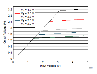
Transfer Characteristics of an N-Channel Transistor

4 Revision History
Changes from * Revision (May 2014) to A Revision