DLPU018J October 2014 – June 2024 DLPC900
- 1
- Read This First
- 1Interface Protocol
-
2DLPC900 Control Commands
- 2.1 DLPC900 Status Commands
- 2.2 DLPC900 Firmware Programming Commands
- 2.3
Chipset Control Commands
- 2.3.1 Chipset Configuration Commands
- 2.3.2 Parallel Interface Configuration
- 2.3.3 Input Source Commands
- 2.3.4 Image Flip
- 2.3.5 IT6535 Power Mode
- 2.3.6 Gamma Configuration and Enable
- 2.3.7 LED Driver Commands
- 2.3.8 GPIO Commands
- 2.3.9 Pulse Width Modulated (PWM) Control
- 2.3.10 Batch File Commands
- 2.4 Display Mode Commands
- 2.5 Debug Mode Commands
- 3DLPC900 Fault Status
- 4Power-Up and Power-Down and Initialization Considerations
- 5Command Examples
- A Register Quick Reference
- B Batch File Command Descriptors
- C Revision History
2.4 Display Mode Commands
The DLPC900 display consists of several parameters which dictate the loading of the DMD and the control of PWM to the LEDs. The DLPC900 supports four main display modes:
- Video Mode
- Video Pattern Mode
- Pre-Stored Pattern Mode
- Pattern On-The-Fly Mode
The Display Mode Selection command (Section 2.4.1) selects between these modes.
In Video mode, the DLPC900 30-bit RGB interface supports up to the native resolution of the attached DMD. The DLPC900 processes the digital input image and converts the data into the appropriate format.
The DLPC900 offers scaling and cropping functions to appropriately display resolutions on single controller DMDs.
The DLPC900 combined with dual controller DMDs does not support scaling or cropping functions.
In the latter three modes, the DLPC900 provides high-speed pattern rates. These modes support only 24-bit data input through the DLPC900 RGB interface (Video Pattern Mode), from flash memory (Pre-Stored Pattern Mode), or dynamically loaded (Pattern On-The-Fly Mode). These modes are well-suited for techniques such as structured light, additive manufacturing, or digital exposure. The DLPC900 also has the capability to display a set of patterns and signal a camera to capture when these patterns are displayed.
Figure 2-4 shows the DLPC900 Single Controller DMD block diagram and Figure 2-5 shows the DLPC900 Dual Controller DMD block diagram. The main functional blocks for the four display modes are shown in these diagrams.
 Figure 2-4 DLPC900
Single Controller System Block Diagram
 Figure 2-5 DLPC900 Dual Controller System
Block Diagram
Figure 2-5 DLPC900 Dual Controller System
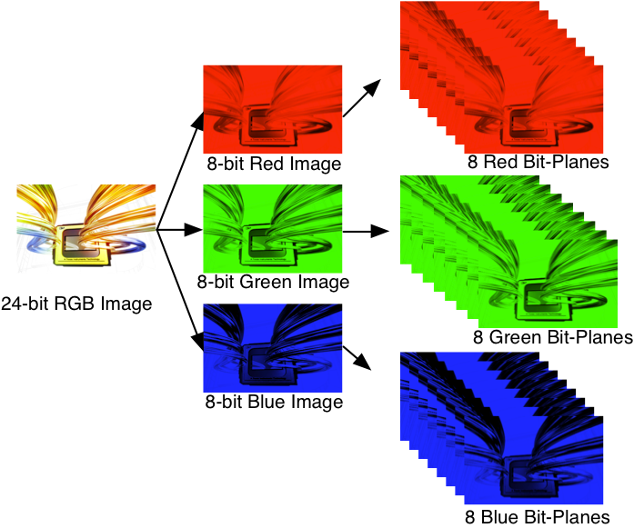
Block DiagramIn Video mode, the DLPC900 operates on a per-frame basis where it takes the input data and appropriately allocates it in a frame. For example, a 24-bit RGB input image is allocated into a 60-Hz frame by dividing each color (red, green, and blue) into specific percentages of the frame. Therefore, for a 40% red, 45% green, and 15% blue ratio, results in the red, green, and blue colors having a 6.67-, 7.5-, and 2.54-ms time slot allocated, respectively. Because each color has an 8-bit depth, each color time slot is further divided into bit-planes, as shown in Figure 2-6. A bit-plane is the two-dimensional arrangement of one bit extracted from all the pixels in the full color 2D image.
 Figure 2-6 Bit-Planes of a 24-Bit RGB Image
The length of each bit-plane in the time slot is weighted by the corresponding power of two of its binary representation resulting in a binary pulse-width modulation of the image. For example, a 24-bit RGB input has three colors with 8-bit depth each. Each color time slot is divided into eight bit-planes, with the sum of the weight of all bit planes in the time slot equal to 255. See Figure 2-7 for an illustration of this partition of the bits in a frame.
 Figure 2-7 Bit
Partition in a Frame for an 8-Bit Monochrome Image
Figure 2-7 Bit
Partition in a Frame for an 8-Bit Monochrome ImageTherefore, a single video frame is composed of a series of bit-planes. Because the DMD mirrors can be either on or off, an image is created by turning on the mirrors corresponding to the bit set in a bit-plane. With binary pulse width modulation, the intensity level of the color is reproduced by controlling the amount of time the mirror is on. For a 24-bit RGB frame image inputted to the DLPC900 controller, the DLPC900 controller creates 24 bit-planes, stores them in internal embedded DRAM, and sends them to the DMD, one bitplane at a time. The bit weight controls the illumination intensity of the bit-plane where smaller the bit weight is the less intense the bit-plane becomes. To improve image quality in video frames, these bit-planes, time slots, and color frames are shuffled and interleaved within the pixel processing functions of the DLPC900 controller.
For other applications where one-to-one pixel mapping to the DMD micromirror is required, the scaling, cropping, and pixel processing functions are disabled and a specific set of patterns is used. The bit-depth of the pattern is then allocated into the corresponding binary weighted time slots. Furthermore, output trigger signals are also synchronized with these time slots to indicate when the image is displayed. For structured light applications, this mechanism provides the capability to display a set of patterns and signal a camera to capture these patterns overlaid on an object.