DLPU094 July 2020 DLP5530S-Q1
7.3.1.1 Video Path
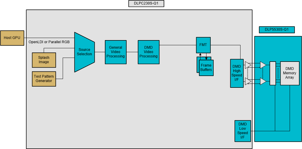
Figure 6 shows the video path of the DLP5530S-Q1.
 Figure 6. DLP5530S-Q1 Video Path
 The DLPC230S-Q1 can use several display sources. Source video can come from a vehicle's GPU, either using OpenLDI or Parallel RGB, Internal Test Patterns, or Splash Images. The video source is selected by a host MCU.
After the input multiplexer, some general video processing is applied to the video. This processing includes scaling, and color space correction (for some splash images). Next, some DMD specific video processing is applied. This includes de-gamma correction, dithering, and finally, a conversion to single color "bit plane" data.
"Bit Planes" are sub-frames corresponding to single color codes. The DMD displays single color sub-frames and the human eye integrates them to form a full color image for that frame of the video. After conversion from standard video to bit planes the video is sent to the FMT block.
The FMT consists of some video processing logic and is connected to two frame buffers. The processing in the FMT and the use of the frame buffers is explained below:
- Performs flips, crops, and bezel adjustment of the video. This video is stored into one of the two frame buffers.
- Simultaneously, video from the other frame buffer is output to the DMD.
- The two frame buffers switch roles every frame.
The DMD High Speed Interface is used to load time multiplexed binary data into the DMD's Memory Array. This binary data determines the state of each DMD mirror during each "bit plane". A reset pulse transitions micro-mirrors from one "bit plane" to the next. The DLPC230S-Q1 utilizes a low speed interface that is used for configuration of DMD registers, generating the DMD mirror reset waveforms, and monitoring the DMD.
The DLP5530S-Q1 chipset contains overlapping BIST coverage of the various blocks involved in the video path. These BISTs cover the input, processing, and output of the video path. These BISTs are discussed in the following sections.