Reducing effects of external RC filter circuit on gain and drift error for integrated analog front ends (AFEs): ±10V
| Input | ADC Input | Digital Output |
|---|---|---|
| VinMin = –10V | AIN-xP = –10V, AIN-xGND = 0V | –3276810, 8000H |
| VinMax = 10V | AIN-xP = 10V AIN-xGND = 0V | 3276710, 7FFFH |
| Power Supplies | |
|---|---|
| AVDD | DVDD |
| 5V | 5V |
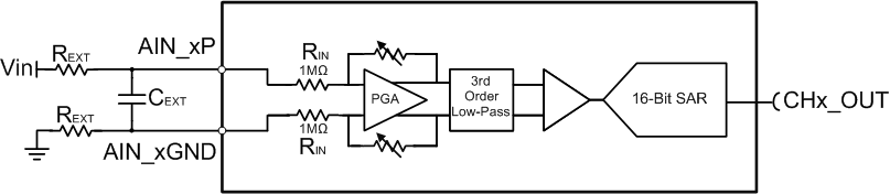
Design Description
This cookbook design describes how to select filter component values and how to minimize the gain error and drift introduced by this filter on a fully-integrated analog front end (AFE) SAR ADC. The design uses the input impedance drift at the full scale range of ±10V of the ADS8588S. This external RC filter minimizes external noise and provides protection from electrical overstress. Minimizing gain error and drift are important to end equipment such as: Multi-Function Relays, AC Analog Input Modules, and Terminal Units. This design describes two correction methods, a no-calibration correction factor and a 2-point calibration. Implementing calibration can minimize both the gain error introduced by the external resistor and the internal device gain error to negligible levels.
Specifications
| Specification | Calculated | Measured |
|---|---|---|
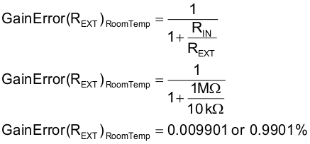
| Introduced Gain Error (25°C) | 0.9901% | 0.9894% |
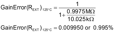
| Introduced Gain Error (125°C) | 0.995% | –1.1388% |
| Introduced Gain Error Drift | 0.49ppm/°C | –0.8031ppm/°C |
Design Notes
- Use low drift REXT resistors to maintain low drift and minimize gain error. This design uses resistors with a temperature coefficient of 25ppm/°C and ±0.1% tolerance.
- The internal programmable gain amplifier (PGA) presents a constant resistive impedance of 1MΩ.
- The REXT value introduced is directly proportional to the introduced error.
- Calibration can also be used to eliminate system offset gain error.
- The TI Precision Labs – ADCs training video series covers methods for calculating gain and offset error and eliminating these errors through calibration, see Understanding and Calibrating the Offset and Gain for ADC Systems. Using SPICE Monte Carlo Tool for Statistical Error Analysis explains how to use Monte Carlo Analysis for statistical error analysis.
Component Selection
External anti-aliasing RC filters reduce noise and protect from electrical overstress; if a large resistor value is used, then this further limits the input current. A large external resistive value also provides a low cutoff frequency, which is desired for relay protection applications as the input frequencies are usually 50 or 60Hz. Furthermore, a balanced RC filter configuration is required for better common-mode noise rejection; matching external resistors are present on both the negative and positive input paths. To minimize the introduced drift error, the external resistors needs to be low drift; 25ppm/°C resistors.
- Choose a high-value REXT
based on the desired cutoff frequency. A cutoff frequency of 320Hz was used to
eliminate harmonics from a 50 or 60Hz input signal.
REXT = 10kΩ
- Choose
CEXT
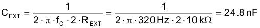
Nearest standard capacitor value available, CEXT = 24nF
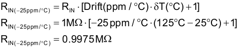
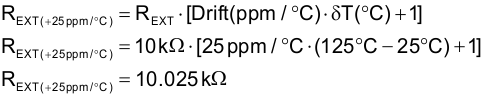
Calculate Gain Error Drift
This section demonstrates how to calculate the introduced gain error drift. The additional drift from the external filter resistor is small compared to the internal device drift.
- Calculate effective internal impedance due to maximum negative
drift (–25ppm/°C)
- Calculate effective external resistance due to maximum positive
drift (25ppm/°C)
- Calculate nominal gain error introduced by the external resistor
at room temperature
- Calculate nominal gain error introduced by the external resistor
at highest rated temperature
- Calculate gain error drift introduced by the external resistor
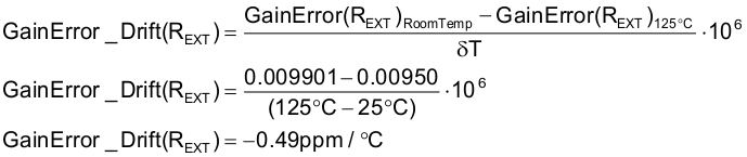
The maximum gain error temperature drift of the ADS8588S is ±14ppm/°C, which is orders of magnitude larger than the calculated drift error introduced, making the introduced error negligible. The minimal drift error introduced by the external resistors has greatly to do with the low drift coefficient of the input impedance (±25ppm/⁰C).
To measure the introduced gain error drift, two test signals are sampled and applied at 0.5V from the full scale input range within the linear range of the ADC. The signals are applied and sampled with and without the external RC filter present. These measurements are performed at both temperatures, 25°C and 125°C. The percent gain errors are solved for by finding the percent error of the ideal slope and the measured slope for each of the four distinctive test conditions, resulting in four distinct percent gain error measurements. The drift (ppm/°C) with and without the RC present is then calculated by converting the percent gain errors to decimal format then following step 5 shown above. The introduced gain error drift is then solved for by subtracting the drift of the RC and no RC present.
Uncalibrated Correction
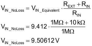
An uncalibrated correction targets to solve the input voltage before any losses occur due to the RC filter by working backwards from the ADC measured samples using a voltage divider.
- Apply known test signal and measure equivalent code
Vin Measured Code Equivalent Measured Input 9.5V 30841 9.412 - Calculate the input voltage before RC losses
Uncalibrated Correction Measurements
Using a voltage correction can be beneficial, but not the most comprehensive. The correction factor can have a worst-case error of 0.2456% at room temperature due to change in internal impedance.
| Room Temperature (25°C) Measurements | ||||
|---|---|---|---|---|
| Vin | Code | Reading | Correction | Error % |
| 9.5 | 30841 | 9.412 | 9.506120 | 0.0644 |
| 8.5 | 27594 | 8.421 | 8.505210 | 0.0613 |
| 5 | 16232 | 4.954 | 5.003540 | 0.0708 |
| 0 | 1 | 0 | 0.000000 | – |
| –5 | –16230 | –4.953 | –5.002530 | 0.0506 |
| –8.5 | –27593 | –8.421 | –8.505210 | 0.0613 |
| –9.5 | –30839 | –9.411 | –9.505110 | 0.0538 |
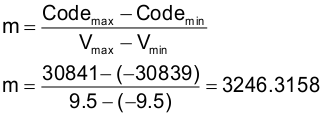
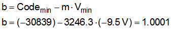
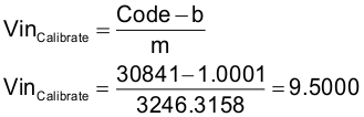
2-Point Calibration Method
A two point calibration applies and samples two test signals at 0.5V from the full scale input range within the linear range of the ADC. These sample measurements are then used to calculate the slope and offset of the linear transfer function. Calibration eliminates both the gain error introduced by the external resistor and the internal device gain error.
- Apply test signal at 2.5% of input linear range
Vmin Measured Code –9.5V –30839 - Apply test signal at 97.5% of input linear range
Vmax Measured Code 9.5V 30841 - Calculate slope and offset calibration coefficients
- Apply calibration coefficient to all subsequent measurements
2-Point Calibration Method Measurements
Calibration Coefficients
m = 3246.3158; b = 1.0001
At room temperature without calibration, a gain error is present. Once calibration is applied to the measured results from the ADC, the gain error is minimized to nearly zero.
| Room Temperature (25°C) Measurements | |||||
|---|---|---|---|---|---|
| VIN | Code | Uncalibrated VIN | Calibrated VIN | Voltage Error Without Calibration % | Voltage Error With Calibration % |
| 9.5 | 30841 | 9.412 | 9.500000 | –0.926316 | –0.000001 |
| 8.5 | 27594 | 8.421 | 8.499789 | –0.929412 | –0.002480 |
| 5 | 16232 | 16232 | 4.999822 | –0.920000 | –0.003568 |
| 0 | 1 | 0 | 0.000000 | – | – |
| –5 | –16230 | –4.953 | –4.999822 | –0.0940000 | –0.003567 |
| –8.5 | –27593 | –8.421 | –8.500097 | –0.929412 | 0.001144 |
| –9.5 | –30839 | –9.411 | –9.500000 | –0.936842 | 0.000000 |
When exposed to high temperatures, the gain error increases, as expected. Once calibration is applied, the voltage error is decreased but not eliminated; the error still present is the drift error.
| High Temperature (125°C) Measurements | |||||
|---|---|---|---|---|---|
| VIN | Code | Uncalibrated VIN | Calibrated VIN | Relative Voltage Error Without Calibration % | Relative Voltage Error With Calibration % |
| 9.5 | 30826 | 9.407 | 9.495379 | –0.978947 | –0.048639 |
| 8.5 | 27582 | 8.417 | 8.496093 | –0.976471 | –0.045968 |
| 5 | 16224 | 4.951 | 4.997357 | –0.980000 | –0.052854 |
| 0 | 0 | 0 | –0.000308 | 0 | – |
| –5 | –16224 | –4.951 | –4.997973 | –0.980000 | –0.040531 |
| –8.5 | –27581 | –8.417 | –8.496401 | –0.976471 | –0.042344 |
| –9.5 | –30826 | –9.407 | –9.495995 | –0.978947 | –0.042153 |
Design References
See Analog Engineer's Circuit Cookbooks for TI's comprehensive circuit library.
Design Featured Devices
| Device | Key Features | Link | Similar Devices |
|---|---|---|---|
| ADS8588S | 16-bit, high-speed 8-channel simultaneous-sampling ADC with bipolar inputs on a single supply | www.ti.com/product/ADS8588S | www.ti.com/adcs |
Trademarks
All trademarks are the property of their respective owners.
IMPORTANT NOTICE AND DISCLAIMER
TI PROVIDES TECHNICAL AND RELIABILITY DATA (INCLUDING DATASHEETS), DESIGN RESOURCES (INCLUDING REFERENCE DESIGNS), APPLICATION OR OTHER DESIGN ADVICE, WEB TOOLS, SAFETY INFORMATION, AND OTHER RESOURCES “AS IS” AND WITH ALL FAULTS, AND DISCLAIMS ALL WARRANTIES, EXPRESS AND IMPLIED, INCLUDING WITHOUT LIMITATION ANY IMPLIED WARRANTIES OF MERCHANTABILITY, FITNESS FOR A PARTICULAR PURPOSE OR NON-INFRINGEMENT OF THIRD PARTY INTELLECTUAL PROPERTY RIGHTS.
These resources are intended for skilled developers designing with TI products. You are solely responsible for (1) selecting the appropriate TI products for your application, (2) designing, validating and testing your application, and (3) ensuring your application meets applicable standards, and any other safety, security, or other requirements. These resources are subject to change without notice. TI grants you permission to use these resources only for development of an application that uses the TI products described in the resource. Other reproduction and display of these resources is prohibited. No license is granted to any other TI intellectual property right or to any third party intellectual property right. TI disclaims responsibility for, and you will fully indemnify TI and its representatives against, any claims, damages, costs, losses, and liabilities arising out of your use of these resources.
TI’s products are provided subject to TI’s Terms of Sale (www.ti.com/legal/termsofsale.html) or other applicable terms available either on ti.com or provided in conjunction with such TI products. TI’s provision of these resources does not expand or otherwise alter TI’s applicable warranties or warranty disclaimers for TI products.
Mailing Address: Texas Instruments, Post Office Box 655303, Dallas, Texas 75265
Copyright © 2024, Texas Instruments Incorporated