SBAA242B December 2017 – September 2024 ADS8900B , ADS8910B , OPA320
| Input | ADC Input | Digital Output ADS8910 | ||||
|---|---|---|---|---|---|---|
| VinMin = –20V | VoutDif = 4.8V, VoutP = 4.9V, VoutN = 0.1V | 1EB85H or 12582910 | ||||
| VinMax = 20V | VoutDif = –4.8V, VoutP = 0.1V, VoutN = 4.9V | 2147BH or –12582910 | ||||
| Vcc | Vee | Vref | Vcm |
|---|---|---|---|
| 5.3V | 0V | 5V | 2.5V |
Design Description
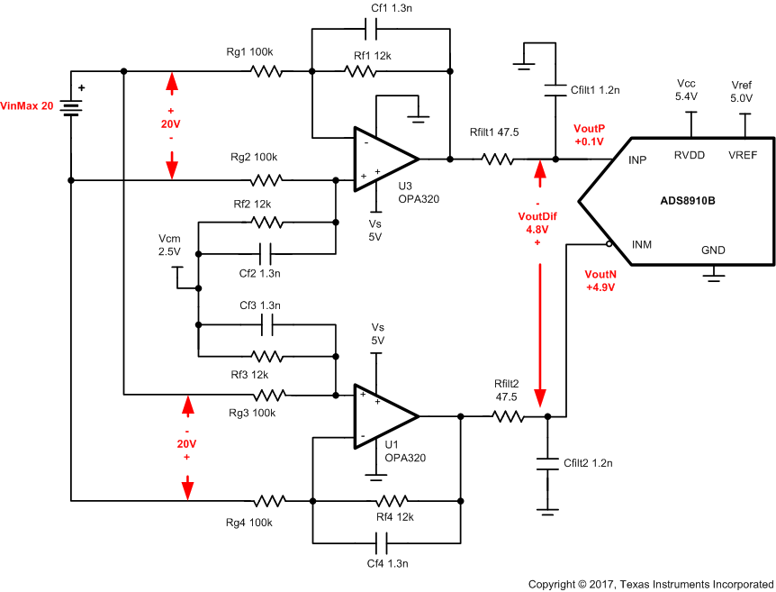
This design translates an input bipolar signal of ±20V into a fully differential ADC differential input scale of ±4.8V, which is within the output linear operation of amplifiers. The values in the component selection section can be adjusted to allow for different input voltage levels.
This circuit implementation is applicable in accurate voltage measurement applications such as Battery Maintenance Systems, Battery Analyzers, battery cell formation and test equipment, ATE, and Remote Radio Units (RRU) in wireless base stations.
Specifications
| Specification | Calculated | Simulated | Measured |
|---|---|---|---|
| Transient ADC Input Settling | < 0.5LSB or 19µV | 6.6µV | N/A |
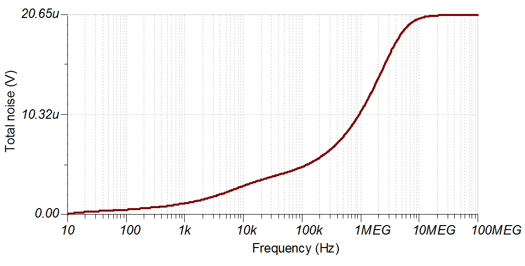
| Noise | 20.7µVrms | 20.65µVrms | 30.8µVrms |
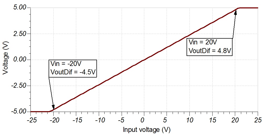
| Bandwidth | 10.2kHz | 10.4kHz | 10.4kHz |
Design Notes
- Determine the linear range of the op amp based on common mode, output swing, and linear open-loop gain specification. This is covered in the component selection section.
- For capacitors in the signal path, select COG type to minimize distortion. In this circuit Cf1, Cf2, Cf3, Cf4, Cfilt1, and Cfilt2 need to be COG type.
- Use 0.1% 20ppm/°C film resistors or better for good gain drift and to minimize distortion.
- Precision labs video series covers methods for error analysis. Review the Statistics Behind Error Analysis for methods to minimize gain, offset, drift, and noise errors.
- The TI Precision Labs – ADCs training video series covers methods for selecting the charge bucket circuit Rfilt and Cfilt. These component values are dependent on the amplifier bandwidth, data converter sampling rate, and data converter design. The values shown here will give good settling and AC performance for the amplifier, gain settings, and data converter in this example. If the design is modified, select a different RC filter. Refer to Introduction to SAR ADC Front-End Component Selection for an explanation of how to select the RC filter for best settling and AC performance.
Component Selection
- The general equation for this
circuit.
- Find op amp maximum and minimum
output for linear operation.
- Rearrange the equation from part 1
and solve for VoutDifMin and VoutDifMax. Find maximum and minimum differential
output voltage based on combined worst case from step2.
- Find differential gain based on
results from step 3.
- Find standard resistor values for
differential gain. Use Analog Engineer's Calculator ("Amplifier and
Comparator\Find Amplifier Gain" section) to find standard values for Rf/Rg
ratio.
- Find Cf for cutoff frequency.
DC Transfer Characteristics
The following graph shows a linear output response for inputs from –20V to +20V. Refer to Determining a SAR ADC’s linear range when using operational amplifiers for detailed theory on this subject.
AC Transfer Characteristics
The bandwidth is simulated to be 10.4 kHz, and the gain is –12.4dB which is a linear gain of 0.12. See Op Amps: Bandwidth 1 for more details on this subject.
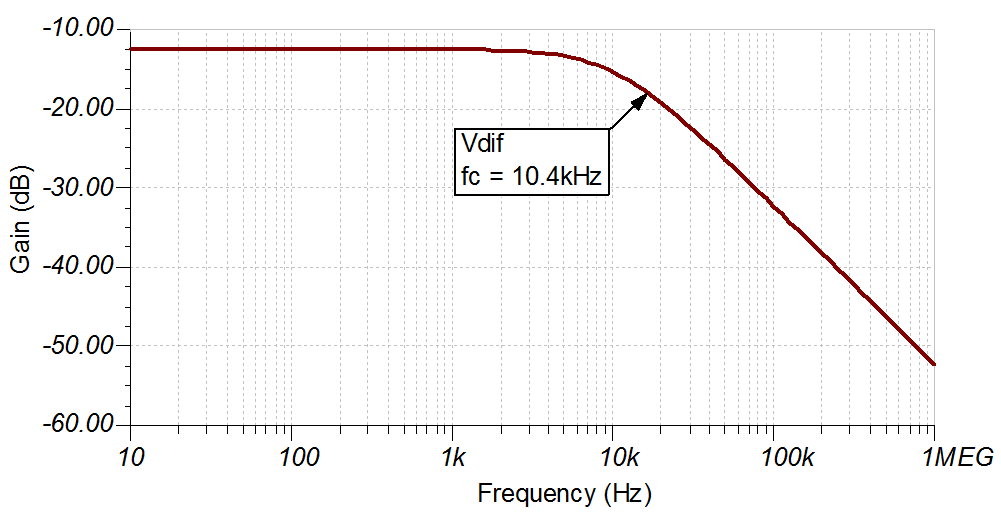
Transient ADC Input Settling Simulation
The following simulation shows settling to a –20V dc input signal. This type of simulation shows that the sample and hold kickback circuit is properly selected. Refer to Introduction to SAR ADC Front-End Component Selection for detailed theory on this subject.
Noise Simulation
The following simplified noise calculation is provided for a rough estimate. We neglect resistor noise in this calculation as it is attenuated for frequencies greater than 10kHz.
Note that calculated and simulated match well. Refer to Calculating the Total Noise for ADC Systems for detailed theory on this subject.
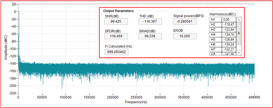
Measure FFT
This performance was measured on a modified version of the ADS8910BEVM. The AC performance indicates SNR = 99.4dB, and THD = –116.4dB. See Introduction to Frequency Domain for more details on this subject.
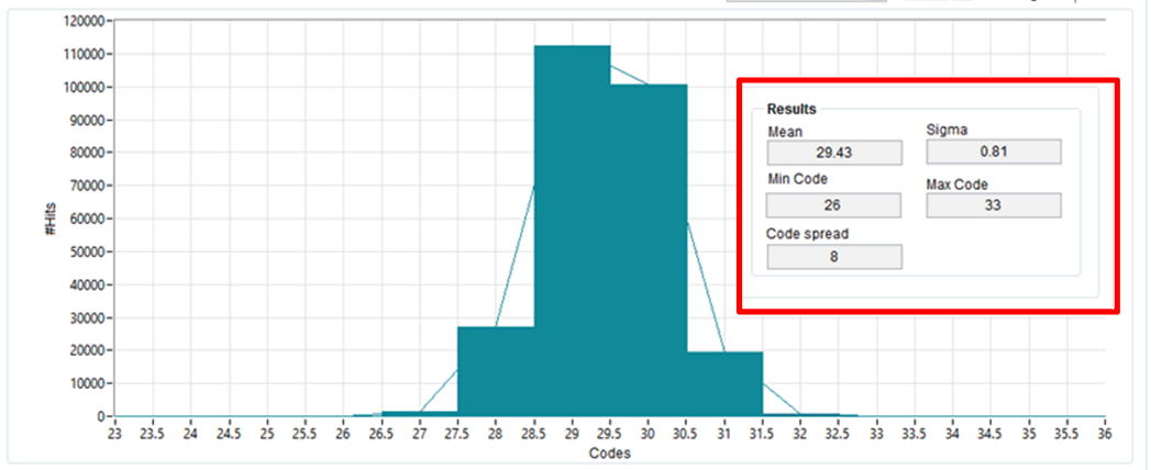
Noise Measurement
The following measured result is for both inputs connected to ground. The histogram shows the system offset and noise. The standard deviation in codes is given by the EVM GUI (0.81), and this can be used to calculate the RMS noise (30.9µV rms) as shown in the following equation.
Design Featured Devices
| Device | Key Features | Link | Similar Devices |
|---|---|---|---|
| ADS8900B(1) | 18-bit resolution, 1-Msps sample rate, Integrated reference buffer, fully differential input, Vref input range 2.5V to 5V. | 20-bit, 1MSPS, one-channel SAR ADC with internal VREF buffer, internal LDO and enhanced SPI | Precision ADCs |
| OPA320(2) | 20-MHz bandwidth, Rail-to-Rail with Zero Crossover Distortion, VosMax = 150µV, VosDriftMax = 5uV/°C, en = 7nV/rtHz | Precision, zero-crossover, 20MHz, 0.9pA Ib, RRIO, CMOS operational amplifier | Precision op amps (Vos<1mV) |
| REF5050(3) | 3ppm/°C drift, 0.05% initial accuracy, 4µVpp/V noise | 5V, 3µVpp/V noise, 3ppm/°C drift precision series voltage reference | Voltage references |
Link to Key Files for High Voltage Battery Monitor
Texas Instruments, SBAC171 design files, software support