SBAA243A December 2017 – August 2024 ADS8900B , ADS8910B , INA240 , OPA320 , REF5050 , THS4551
| Sense Resistor Current | INA Out, Amplifier Input | ADC Input | Digital Output ADS8910B |
|---|---|---|---|
| MinCurrent = ±50mA | Out = ±10mV | VoutDif = ±21.3mV | 233H 56310, 3FDCBH -5640 |
| MaxCurrent = +10A | Out = ±2V | VoutDif = ± 4.3V | 1B851H 11272210 247AEH -11272210 |
| Vs | Vee | Vref | Vcm |
|---|---|---|---|
| 5.3 V <Vs <5.5V | 0V | 5V | 2.5V |
Design Description
This single-supply current sensing solution can measure a current signal in the range of ±50 mA to ±10 A across a shunt resistor. The current sense amplifier can measure shunt resistors over a wide common-mode voltage range from 0V to 75V. A fully differential amplifier (FDA) performs the single-ended to differential conversion and drives the SAR ADC differential input scale of ±5V at full data rate of 1MSPS. The values in the component selection section can be adjusted to allow for different current levels.
This circuit implementation is applicable in accurate voltage measurement applications such as battery maintenance systems, battery analyzers, battery cell formation and test equipment, automatic test equipment, and Remote Radio Units (RRU) in wireless base stations.
| Error Analysis | Calculated | Simulated | Measured |
|---|---|---|---|
| Transient ADC Input Settling | > 1LSB > 38µV | 6.6µV | N/A |
| Noise (at ADC Input) | 221.8µV rms | 207.3µV rms | 227µV rms |
| Bandwidth | 10.6kHz | 10.71kHz | 10.71kHz |
Design Notes
- Determine the shunt sense resistor value and select the current sense amplifier based on the input current range and input common mode voltage requirements. This is covered in the component selection section.
- Determine the fully differential amplifier gain based on the current sense amplifier output, the ADC full-scale range input and the output swing specifications of the fully differential amplifier. This is covered in the component selection section.
- Select COG capacitors to minimize distortion.
- Use 0.1% 20ppm/°C film resistors or better for good accuracy, low gain drift, and to minimize distortion.
- The TI Precision Labs training video series covers methods for error analysis. Review the following links for methods to minimize gain, offset, drift, and noise errors: Error and Noise.
- The TI Precision Labs – ADCs training video series covers methods for selecting the charge bucket circuit Rfilt and Cfilt. These component values are dependent on the amplifier bandwidth, data converter sampling rate, and data converter design. The values shown here will give good settling and ac performance for the amplifier, gain settings, and data converter in this example. If the design is modified, select a different RC filter. Refer to Introduction to SAR ADC Front-End Component Selection for an explanation of how to select the RC filter for best settling and ac performance.
Component Selection for Current Sense Circuit
- Choose the Rsense resistor and find
the gain for the current sense amplifier (bidirectional current).
- Calculate the current sense
amplifier output range.
- Find ADC full-scale input range and
results from step 3.
- Find FDA maximum and minimum output
for linear operation.
- Find differential gain based on ADC
full-scale input range, FDA output range and results from step 3.
- Find standard resistor values for
differential gain.
- Find RfINA,
CfINA for cutoff frequency.
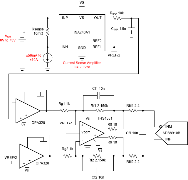
Fully Differential DC Transfer Characteristics
The following graph shows a linear output response for inputs from –10A to +10A.
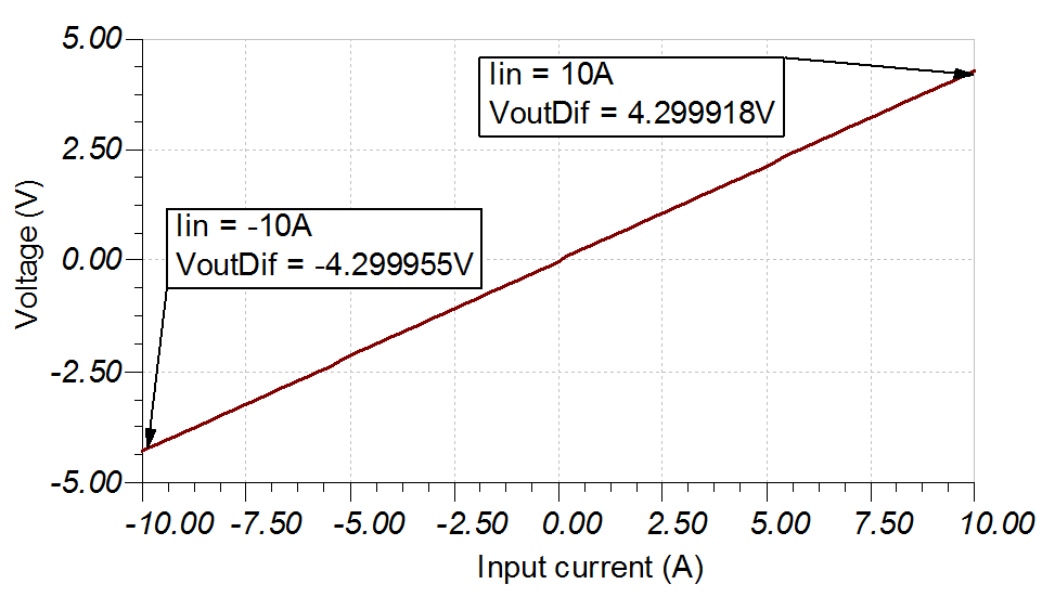
AC Transfer Characteristics
The bandwidth is simulated to be 10.5kHz and the gain is 32.66dB which is a linear gain of 43V/V (G = 20×2.15V/V).
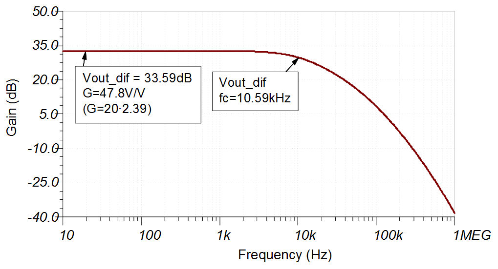
Noise Simulation
The following simplified noise calculation is provided for a rough estimate. Since the current sense amplifier INA240 is the dominant source of noise, the noise contribution of the OPA320 buffers and THS4521 is omitted in the noise estimate. We neglect resistor noise in this calculation as it is attenuated for frequencies greater than 10.6kHz.
Note that calculated and simulated match well. Refer to Noise - Lab for detailed theory on amplifier noise calculations, and ADC noise measurement, methods and parameters for data converter noise.
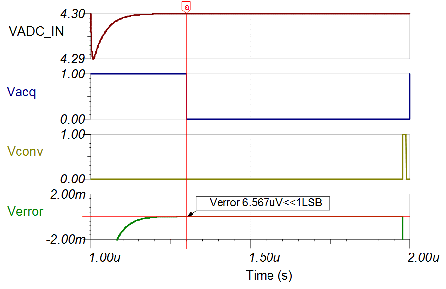
Transient ADC Input Settling Simulation
The following simulation shows settling to a 10-A DC input signal (ADC differential input signal +4.3V). This type of simulation shows that the sample and hold kickback circuit is properly selected. Refer to Final SAR ADC Drive Simulations for detailed theory on this subject.
Design Featured Devices:
| Device | Key Features | Link | Similar Devices |
|---|---|---|---|
| ADS8910B(1) | 18-bit resolution, 1-Msps sample rate, integrated reference buffer, fully differential input, Vref input range 2.5V to 5V | 18-Bit, 1-MSPS, 1-Ch SAR ADC with Internal VREF Buffer, Internal LDO and Enhanced SPI Interface | Precision ADCs |
| INA240 | High- and low-Side, bi-directional, zero-drift current sense amp, GainError = 0.20%, Gain = 20V/V, wide common-mode = –4V to 80V | -4 to 80V, bidirectional, ultra-precise current sense amplifier with enhanced PWM rejection | Instrumentation amplifiers |
| THS4551 | Fully differential amplifier (FDA), 150-MHz bandwidth, Rail-to-Rail output, VosDriftMax = 1.8 µV/°C, en = 3.3 nV/rtHz | Low Noise, Precision, 150MHz, Fully Differential Amplifier | Operational amplifiers (op amps) |
| OPA320 | 20-MHz bandwidth, Rail-to-Rail with zero crossover distortion, VosMax = 150 µV, VosDriftMax = 5 µV/C, en = 7 nV/rtHz | Precision, zero-crossover, 20-MHz, 0.9-pA Ib, RRIO, CMOS operational amplifier | Operational amplifiers (op amps) |
| REF5050 | 3 ppm/°C drift, 0.05% initial accuracy, 4 µVpp/V noise | 5-V, 3-µVpp/V noise, 3-ppm/°C drift precision series voltage reference | Series voltage references |
Link to Key Files
Texas Instruments, ADS8900B Design File, software support