SBAA245B December 2017 – September 2024 ADS8860 , INA826 , OPA192
| Input | ADC Input | Digital Output ADS8860 |
|---|---|---|
| –5mV | Out = 0.2V | 0A3DH or 262110 |
| 15mV | Out = 4.8V | F5C3H or 6291510 |
| AVDD | DVDD | Vref_INA | Vref | Vcc | Vee |
|---|---|---|---|---|---|
| 5.0V | 3.0V | 3.277V | 5.0V | +15V | –15V |
Design Description
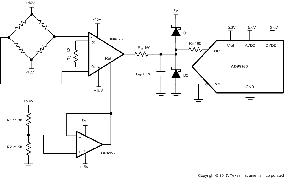
Instrumentation amplifiers are a common way of translating low level sensor outputs to high level signals to drive an ADC. Typically, instrumentation amplifiers are optimized for low noise, low offset, and low drift. Unfortunately, the bandwidth of many instrumentation amplifiers may not be sufficient to achieve good settling to ADC charge kickback at maximum sampling rates. This document shows how sampling rate can be adjusted to achieve good settling. Furthermore, many instrumentation amplifiers are optimized for high-voltage supplies and it may be required to interface the high-voltage output (that is, ±15V) to a lower voltage ADC (for example, 5V). This design shows how to use Schottky diodes and a series resistor to protect the ADC input from an overvoltage condition. Note that the following circuit shows a bridge sensor, but this method could be used for a wide range of different sensors. A modified version of this circuit, Driving a Switched-Capacitor SAR With a Buffered Instrumentation Amplifier shows how a wide bandwidth buffer can be used to achieve higher sampling rate.
This circuit implementation is applicable to all Bridge Transducers in PLC’s and Analog Input Modules that require precision signal-processing and data-conversion.
Specifications
| Specification | Calculated | Simulated |
|---|---|---|
| Sampling rate | 200ksps | 200ksps, settling to –6µV |
| Offset (ADC Input) | 40µV × 306.7 = 12.27mV | 16mV |
| Offset Drift | (0.4µV/°C) × 306.7 = 123µV/°C | NA |
| Noise | 978µV | 874µV |
Design Notes
- Select the gain to achieve an input swing that matches the input range of the ADC. Use the instrumentation amplifier reference pin to shift the signal offset to match the input range. This is covered in the component selection section.
- The input Schottky diode configuration is used to prevent driving the input voltage outside of the absolute maximum specifications. The BAT54S Schottky is a good option for design as this device integrates both diodes into one package and the diodes are low leakage and have a low forward voltage. This is covered in the component selection section.
- The buffer amplifier following the voltage divider is required for driving the reference input of most instrumentation amplifiers. Choose precision resistors and a precision low-offset amplifier as the buffer. Refer to Selecting the right op amp for more details on this subject.
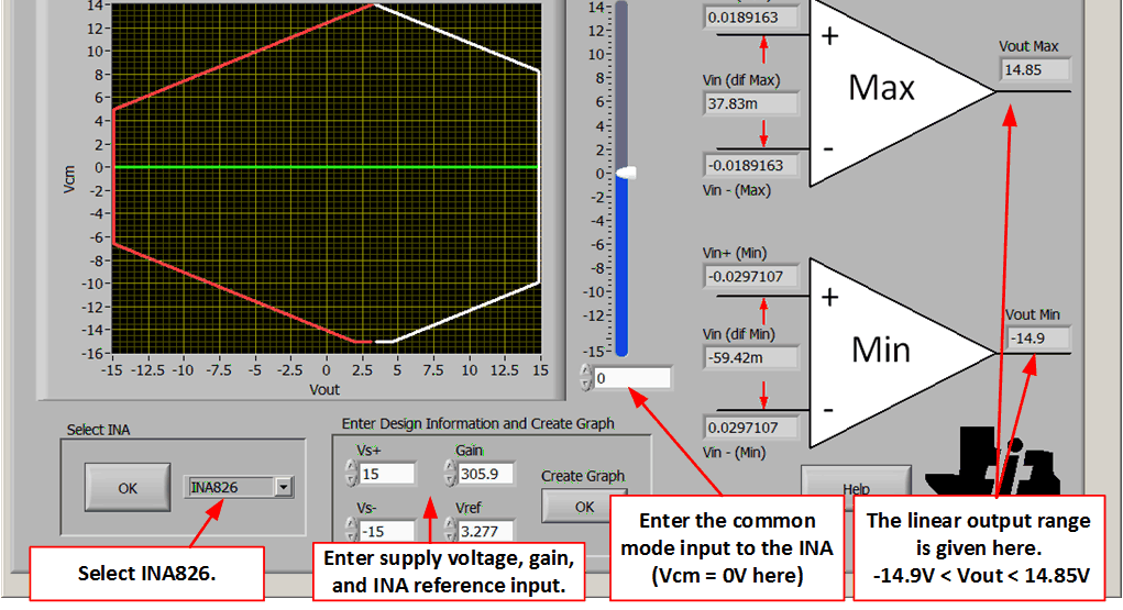
- Check the common-mode range of the amplifier using the Common-Mode Input Range Calculator for Instrumentation Amplifiers software tool.
- Select C0G capacitors for CCM1, CCM2, CDIF, and Cfilt to minimize distortion.
- Use 0.1% 20ppm/°C film resistors or better for the gain set resistor Rg. The error and drift of this resistor directly translates into gain error and gain drift.
- The TI Precision Labs – ADCs training video series covers methods for selecting the charge bucket circuit Rfilt and Cfilt. Although this method was designed for op amps, it can be modified for instrumentation amplifiers. Refer to Introduction to SAR ADC Front-End Component Selection for details on this subject.
Component Selection
- Find the gain set resistor for the
instrumentation amplifier to set the output swing to 0.2V to 4.8V.

- Find the INA826 reference voltage
(Vref) to shift the output swing to the proper voltage level.

- Select standard value resistors to set the
INA826 reference voltage (Vref = 3.27V). Use Analog
Engineer's Calculator ("Passive\Find Voltage Divider" section) to find
standard values for the voltage divider.


- Use the Common-Mode Input Range
Calculator for Instrumentation Amplifiers to determine if the INA826 is
violating the common-mode range.
DC Transfer Characteristics
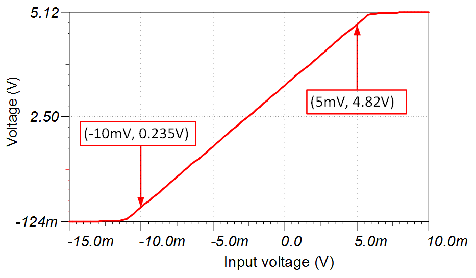
The following graph shows a linear output response for inputs from –5mV to +15mV. Refer to Determining a SAR ADC’s Linear Range when using Instrumentation Amplifiers for detailed theory on this subject. Note that the output range is intentionally limited to –0.12V to 5.12V using Schottky diodes to protect the ADS8860. Note that Schottky diodes are used because the low forward voltage drop (typically less than 0.3V) keeps the output limit very near the ADC supply voltages. The absolute maximum rating for the ADS8860 is –0.3V < Vin < REF +0.3V.
AC Transfer Characteristics
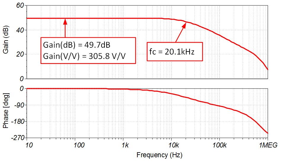
The bandwidth is simulated to be 20.1kHz, and the gain is 49.7dB which is a linear gain of 305.8. See the video series on Op Amps: Bandwidth 1 for more details on this subject.
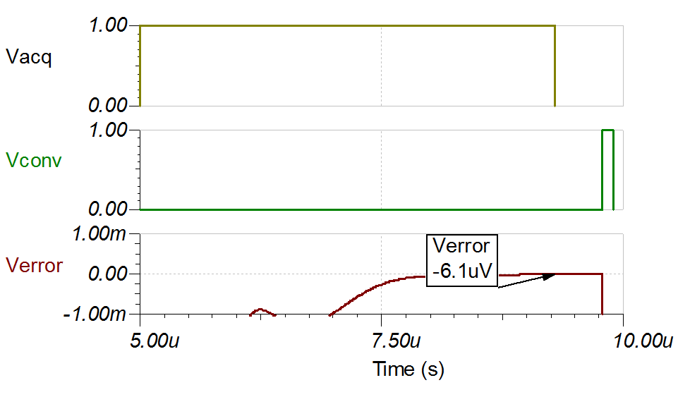
Transient ADC Input Settling Simulation
The following simulation shows settling to a +15mV dc input signal. This type of simulation shows that the sample and hold kickback circuit is properly selected. Refer to Introduction to SAR ADC Front-End Component Selection for detailed theory on this subject
Noise Simulation
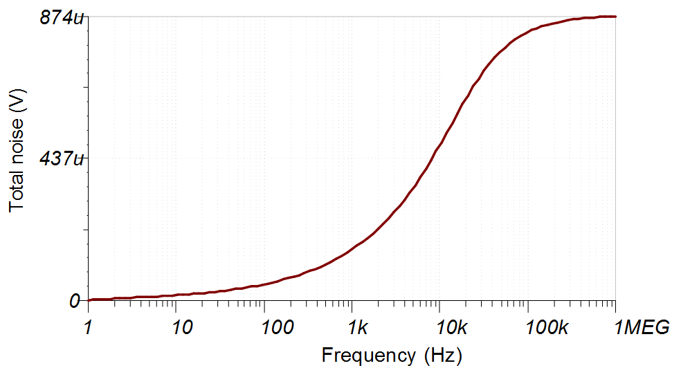
The following simplified noise calculation is provided for a rough estimate. We neglect noise from the OPA192 as the instrumentation amplifier is in high gain, so its noise is dominant.

Note that calculated and simulated match well. Refer to TI Precision Labs - Op Amps: Noise 4 for detailed theory on amplifier noise calculations, and Calculating the Total Noise for ADC Systems for data converter noise.
Optional Input Filter
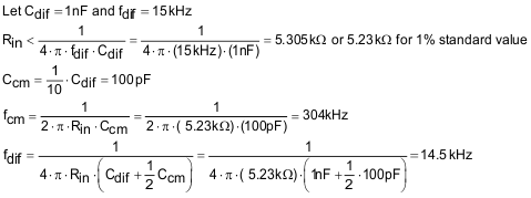
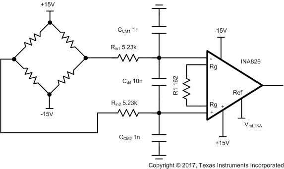
The following figure shows a commonly used instrumentation amplifier input filter. The differential noise is filtered with Cdif, and the common-mode noise is filtered with Ccm1 and Ccm2. Note that it is recommended that Cdif ≥ 10Ccm. This prevents conversion of common-mode noise to differential noise due to component tolerances. The following filter was designed for a differential cutoff frequency of 15kHz.
Design Featured Devices
| Device | Key Features | Link | Similar Devices |
|---|---|---|---|
| ADS8860 | 16-bit resolution, SPI, 1Msps sample rate, single-ended input, Vref input range 2.5V to 5.0V. | 16-bit, 1MSPS, 1-channel SAR ADC with single-ended input, SPI and daisy chain | Precision ADCs |
| OPA192 | Bandwidth 10MHz, Rail-to-Rail input and output, low noise 5.5nV/rtHz, low offset ±5µV, low offset drift ±0.2µV/°C. (Typical values) | High-Voltage, Rail-to-Rail Input/Output, 5µV, 0.2µV/˚C, Precision Operational Amplifier | Precision op amps (Vos<1mV) |
| INA826 | Bandwidth 1MHz (G = 1), low noise 18nV/rtHz, low offset ±40µV, low offset drift ±0.4µV/°C, low gain drift 0.1ppm/°C. (Typical values) | Precision, 200-μA Supply Current, 36-V Supply Instrumentation Amplifier | Instrumentation amplifiers |
Link to Key Files
Texas Instruments, Source Files for SBAA277, support software