SBAA252B February 2018 – September 2024 ADS8900B , OPA320 , TPS7A39
| LDO Input | LDO Output | Output Noise Level |
|---|---|---|
| Vin+ > 6V | 5.2V | 27µVRMS |
| Vin– < –5V | –200mV | 22µVRMS |
Design Description
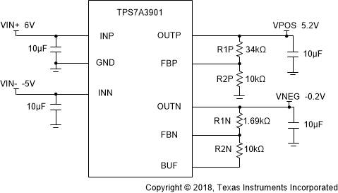
This design shows a power supply that can be used to create a positive operational-amplifier (op amp) supply and a small negative op-amp supply. This small negative voltage is adjustable and is necessary in many operational amplifiers to verify linearity down to ground. This design shows the TPS7A3901 as the power supply for creating the positive and negative voltage rails for operational amplifier circuits. This low dropout regulator (LDO) differs from most in the ability to regulate small negative voltages, as the following image shows. This is a generic circuit implementation that can be used in many Industrial applications.
Specifications
| Parameter | Test Condition | Data Sheet Specification | Measured ADS8900B Performance |
|---|---|---|---|
| SNR | Vin_max = 5V, Vin_min = 0V | 104.5dB | 102.2dB |
| THD | Vin_max = 5V, Vin_min = 0V | –125dB | –123.5dB |
Design Notes
- Determine the linear range of the op amp based on common mode, output swing, and linear open-loop gain specification.
- Set the adjustable LDO outputs to match the linear range of op amp.
- Select X7R capacitors according to the temperature performance.
- In cases where a negative supply is not available, an alternative method is to use a Low Noise Negative Bias Generator (LM7705).
Component Selection
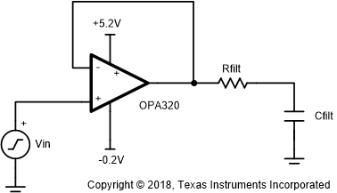
- A common configuration shows in the
following image using an OPA320 in a buffer configuration with a 0V to 5V
desired linear signal swing. The power supplies are both 200mV away from the
desired input and output swing. This topology makes sure of linear input and
output swing for this amplifier.
- Select the components for the
adjustable LDO outputs. Using the previous OPA320 example, the rails for the
system are –200mV and +5.2V.
Desired Output R1 R2 +5.2V 34kΩ 10kΩ –200mV 1.69kΩ 10kΩ
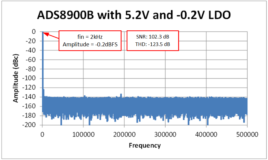
ADS8900B 20-Bit FFT Taken With LDO Adjusted to 5.2V and –0.2V
The FFT in the following was measured with an input signal very near full scale ±5V (–0.2dBFS). Note that the SNR and THD is very good compared to the case where the supply is adjusted to 5V and GND. Note the TPS7A3901 is a convenient way to generate a linear –0.2-V supply.
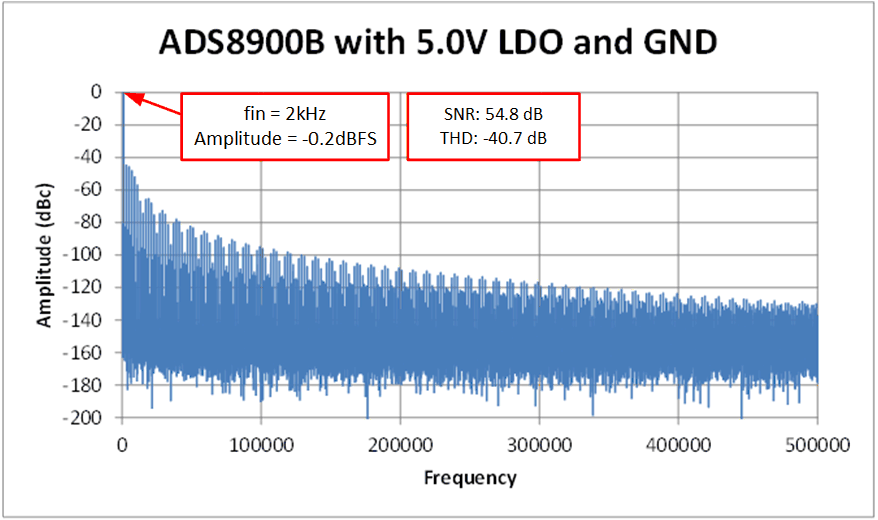
ADS8900B 20-Bit FFT Taken With LDO Adjusted to 5.0V and GND
The FFT shown in the following image was measured with an input signal very near full scale ±5V (–0.2dBFS). Note that the SNR and THD is poor compared to the case where the supply is adjusted to 5.2V and –0.2V.
Design Featured Devices
| Device | Key Features | Link | Similar Devices |
|---|---|---|---|
| TPS7A3901 | The TPS7A39 device is a dual, monolithic, high-PSRR, positive and negative low-dropout (LDO) voltage regulator capable of sourcing (and sinking) up to 150mA of current. The device has a wide output voltage range of 1.2V to 30V for the positive output and –30V to 0V for the negative output. This device is an excellent choice for generating a small negative supply voltage that is useful in cases where a single-supply amplifier needs a small negative supply so that the output can linearly swing to 0V. | www.ti.com/product/TPS7A39 | www.ti.com/product/LM7705(1) |
| ADS8900B | Bipolar differential inputs, SAR ADC with internal reference buffer, SPI interface | www.ti.com/product/ADS8900B | www.ti.com/adcs |
| OPA320 | Precision, Zero-Crossover, 20Mhz, RRIO, CMOS Operational Amplifier | www.ti.com/product/opa320 | www.ti.com/opamp |
Design References
See Analog Engineer's Circuit Cookbooks for TI's comprehensive circuit library.