Low-Power Sensor Measurements: 3.3V, 1kSPS, 12-Bit, Single-Ended, Single-Supply Circuit
| Input | ADC Input | Digital Output ADS7042 |
|---|---|---|
| VinMin = 0V |
AIN_P = 0V, AIN_M = 0V |
000H or 010 |
| VinMax = 3.3V |
AIN_P = 3.3V, AIN_M = 0V |
FFFH or 409610 |
| AVDD | Vee | Vdd |
|---|---|---|
| 3.3V | 0V | 4.5V |
Design Description
This design shows an ultra-low power amplifier being used to drive a SAR ADC that consumes only nanoWatts of power during operation. This design is intended for collecting sensor data by providing overall system-level power consumption on the order of single-digit microWatts. PIR sensors, gas sensors, and glucose monitors are a few examples of possible implementations of this SAR ADC design. The values in the component selection section can be adjusted to allow for different data throughput rates and different bandwidth amplifiers. Low-Power Sensor Measurements: 3.3V, 1ksps, 12-bit Single-Ended, Dual Supply shows a more sophisticated version of this circuit where the negative supply is connected to a small negative voltage (–0.3V). The single-supply version has degraded performance when the amplifier output is near zero volts. However, in most cases the single-supply configuration is preferred for its simplicity.
Specifications
| Specification | Calculated | Simulated | Measured |
|---|---|---|---|
| Transient ADC Input Settling (1ksps) | < 0.5×LSB = 402µV | 41.6µV | N/A |
| AVDD Supply Current (1ksps) | 230nA | N/A | 214.8nA |
| AVDD Supply Power (1ksps) | 759nW | N/A | 709nW |
| VDD OPAMP Supply Current | 450nA | N/A | 431.6nA |
| VDD OPAMP Supply Power | 2.025µW | N/A | 1.942µW |
| AVDD + VDD System Power (1ksps) | 2.784µW | N/A | 2.651µW |
Design Notes
- Determine the linear range of the op amp based on common mode, output swing, and linear open loop gain specification. This is covered in the component selection section.
- Select COG capacitors to minimize distortion.
- Use 0.1% 20ppm/°C film resistors or better to minimize distortion.
- The TI Precision Labs – ADCs training video series covers methods for selecting the charge bucket circuit Rfilt and Cfilt. These component values are dependent on the amplifier bandwidth, data converter sampling rate, and data converter design. The values shown here give good settling and AC performance for the amplifier and data converter in this example. If you modify this design you need to select a different RC filter. Refer to the Introduction to SAR ADC Front-End Component Selection training video for an explanation of how to select the RC filter for best settling and AC performance.
Component Selection
- Select a low-power operational amp:
- Supply current < 0.5µA
- Gain bandwidth product > 5kHz (5 times the sampling rate)
- Unity gain stable
- For this cookbook, the LPV811 was selected. It has a 450-nA supply current, 8-kHz gain bandwidth product, and is unity gain stable.
- Find op amp maximum and minimum
output for linear operation Note: The linear range of the LPV811 is 300mV above ground. This means to design a system to establish a full linear range from 0V to 3.3V (full-scale range (FSR) of ADS7042), then a negative supply is required. This design shows that full-measured SNR and THD specifications of the ADS7042 are met without using a negative supply voltage. This testing was only at room temperature and for a more robust system; Low-Power Sensor Measurements: 3.3V, 1ksps, 12-bit Single-Ended, Dual Supply shows this design using a negative supply instead of ground.
- Typical power calculations (at
1ksps) with expected values:
- Typical power calculations (at
1ksps) with measured values:
- Find Rfilt and Cfilt to allow for settling at 1ksps. Refine the Rfilt and Cfilt Values (a Precision Labs video) showing the algorithm for selecting Rfilt and Cfilt. The final value of 200kΩ and 510pF proved to settle to well below ½ of a least significant bit (LSB).
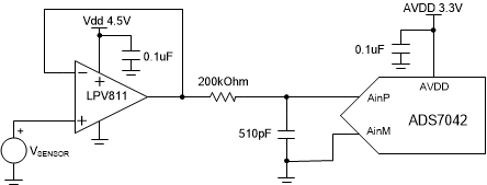
DC Transfer Characteristics
The following graph shows a linear output response for inputs from 0 to 3.3V. The FSR of the ADC falls within the linear range of the op amp.
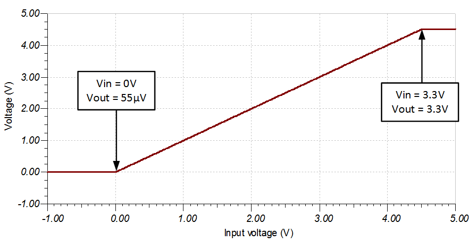
AC Transfer Characteristics
The bandwidth simulation includes the effects of the amplifier output impedance and the RC charge bucket circuit (Rfilt and Cfilt).The bandwidth of the RC circuit is shown in the following equation to be 1.56kHz. The simulated bandwidth of 2kHz includes effects from the output impedance interacting with the impedance of the load. See TI Video Library - Op Amps: Bandwidth 1 for more details on this subject.
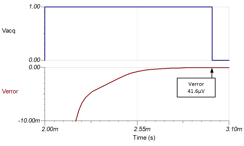
Transient ADC Input Settling Simulation
The following simulation shows settling to a 3-V DC input signal. This type of simulation shows that the sample and hold kickback circuit is properly selected to within ½ of a LSB (402µV). Refer to Introduction to SAR ADC Front-End Component Selection for detailed theory on this subject.
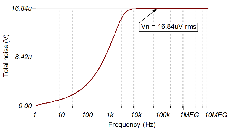
Noise Simulation
This section details a simplified noise calculation for a rough estimate. We neglect resistor noise in this calculation as it is attenuated for frequencies greater than 10kHz.
Note that calculated and simulated match well. Refer to Calculating the Total Noise for ADC Systems for detailed theory on this subject.
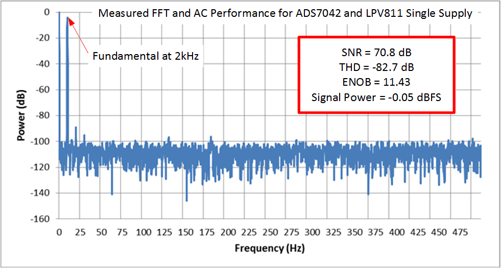
Measure FET
This performance was measured on a modified version of the ADS7042EVM-PDK. The AC performance indicates SNR = 70.8dB, THD = –82.7dB, and ENOB (effective number of bits) = 11.43, which matches well with the specified performance of the ADC of SNR = 70dB.
Design Featured Devices
| Device | Key Features | Link | Similar Devices |
|---|---|---|---|
| ADS7042(1) | 12-bit resolution, SPI, 1-Msps sample rate, single-ended input, AVDD, Vref input range 1.6V to 3.6V. | 12-Bit 1MSPS Ultra-Low-Power Ultra-Small-Size SAR ADC With SPI | ADCS |
| LPV811(2) | 8kHz bandwidth, Rail-to-Rail output, 450nA supply current, unity gain stable | Single Channel 450nA Precision Nanopower Operational Amplifier | Op amp |
Link to Key Files
Texas Instruments, LPV811 TINA files, software download
Revision History
Changes from Revision A (March 2019) to Revision B (September 2024)
- Updated the numbering format for tables, figures, and cross-references throughout the documentGo
Changes from Revision * (February 2018) to Revision A (March 2019)
Trademarks
All trademarks are the property of their respective owners.
IMPORTANT NOTICE AND DISCLAIMER
TI PROVIDES TECHNICAL AND RELIABILITY DATA (INCLUDING DATASHEETS), DESIGN RESOURCES (INCLUDING REFERENCE DESIGNS), APPLICATION OR OTHER DESIGN ADVICE, WEB TOOLS, SAFETY INFORMATION, AND OTHER RESOURCES “AS IS” AND WITH ALL FAULTS, AND DISCLAIMS ALL WARRANTIES, EXPRESS AND IMPLIED, INCLUDING WITHOUT LIMITATION ANY IMPLIED WARRANTIES OF MERCHANTABILITY, FITNESS FOR A PARTICULAR PURPOSE OR NON-INFRINGEMENT OF THIRD PARTY INTELLECTUAL PROPERTY RIGHTS.
These resources are intended for skilled developers designing with TI products. You are solely responsible for (1) selecting the appropriate TI products for your application, (2) designing, validating and testing your application, and (3) ensuring your application meets applicable standards, and any other safety, security, or other requirements. These resources are subject to change without notice. TI grants you permission to use these resources only for development of an application that uses the TI products described in the resource. Other reproduction and display of these resources is prohibited. No license is granted to any other TI intellectual property right or to any third party intellectual property right. TI disclaims responsibility for, and you will fully indemnify TI and its representatives against, any claims, damages, costs, losses, and liabilities arising out of your use of these resources.
TI’s products are provided subject to TI’s Terms of Sale (www.ti.com/legal/termsofsale.html) or other applicable terms available either on ti.com or provided in conjunction with such TI products. TI’s provision of these resources does not expand or otherwise alter TI’s applicable warranties or warranty disclaimers for TI products.
Mailing Address: Texas Instruments, Post Office Box 655303, Dallas, Texas 75265
Copyright © 2024, Texas Instruments Incorporated
