SBAA256B January 2018 – September 2024 ADS7040 , ADS7041 , ADS7042 , ADS7056 , ISOTMP35 , ISOTMP35-Q1
Design Description
This design explains how sensor outputs can be directly interfaced with a SAR ADC input. In applications such as wireless environmental sensors, gas detectors, and smoke and heat detectors, the input is very slow-moving and the sensor output voltage is sampled at fairly slower speeds (10ksps or so). In such or similar systems, the sensor output can be directly interfaced with the SAR ADC input without the need for a driver amplifier to achieve a small form-factor, low-cost design.
Interfacing Sensor Output Directly to a SAR ADC
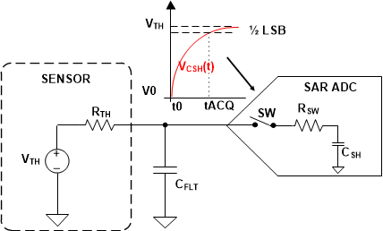
The following figure shows a typical application diagram for interfacing a sensor directly to a SAR ADC input without the use of a driver amplifier. The sensor block highlights the Thevenin equivalent of a sensor output. Voltage source, VTH, is the Thevenin-equivalent voltage and source resistance RTH is the Thevenin-equivalent impedance. Most sensor data sheets provide the Thevenin model of the sensor from which the value of the series impedance can be easily calculated.

Specifications
| Parameter | Calculated | Simulated | Measured |
|---|---|---|---|
| Transient ADC Input Settling Error | <
0.5LSB < 100.5µV |
36.24µV | N/A |
| Step Input Full Scale Range | 3.15V | 3.15V | 3.14978 |
| Input Source Impedance (RTH) | 10kΩ | 10kΩ | 10.01kΩ |
| Filter Capacitor Value (CFLT) | 680pF | 680pF | N/A |
| ADC Sampling Speed | 10ksps | 10ksps | 10ksps |
Design Note
- Determine source impedance of input signal. Calculate the RC time constant of the input source impedance and filter capacitor (known value).
- Determine the minimum acquisition time required for the input signal to settle for a given source impedance and the filter capacitor combination.
- Select COG capacitors to minimize distortion.
- Use 0.1% 20ppm/°C film resistors or better for good gain drift and to minimize distortion.
Component Selection for ADC Input Settling
SAR ADCs can be directly interfaced with sensors when the analog input source is capable of driving the switched capacitor load of a SAR ADC and settling the analog input signal to within ½ of an LSB within the acquisition time of the SAR ADC. To achieve this, the external RC filter (RTH and CFLT) must settle within the acquisition time (tACQ) of the ADC. The relationship between the ADC acquisition time and RC time constant of the external filter is:
where
- ԎFLT = RTH × CFLT
- k is the single pole time constant for N bit ADC
The following design example values are given in the table on page 1:
K = 11 (Single pole time constant multiplier for 14-bit ADC) – More information is found on pages 96 and 97 of the Analog Engineer’s Pocket Reference Guide e-Book.
Minimum acquisition time required for proper settling is calculated using this equation:
For more information on SAR ADCs and front end design for SAR ADCs, refer to theIntroduction to SAR ADC Front-End Component Selection video.
Transient Input Settling Simulation using TI-TINA
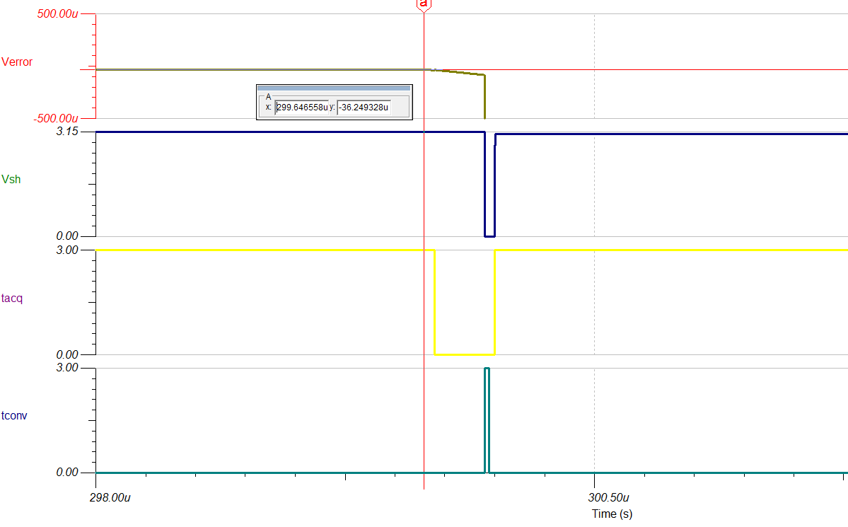
The following figure shows the settling of an ADS7056 ADC given a 3.15-V DC input signal. This type of simulation shows that the sample and hold kickback circuit is properly selected. Refer to Refine the Rfilt and Cfilt Values in the TI Precision Labs - ADCs training video series for detailed theory on this subject.

Increasing Acquisition Time of SAR ADC for Input Signal Settling
The acquisition time of a SAR ADC can be increased by reducing the throughput in the following ways:
- Reducing the SCLK frequency to reduce the throughput.
- Keeping the SCLK fixed at the highest permissible value and increasing the CS high time.
The following table lists the acquisition time for the previous two cases for the ADS7056 SAR ADC operating at 10ksps throughput (tcycle = 100µs). Case 2 provides a longer acquisition time for the input signal to settle because of the increased frequency of the SCLK given a fixed conversion and cycle time.
| Case | SCLK | tcycle | Conversion Time (18 × tSCLK ) | Acquisition Time (tcycle – tconv ) |
|---|---|---|---|---|
| 1 | 0.24MHz | 100µs | 74.988µs | 25.01µs |
| 2 | 60MHz | 100µs | 0.3µs | 99.70µs |
The following table shows a performance comparison between an 8-, 10-, 12-, and 14-bit ADC with respect to sampling speed and effective number of bits (ENOB) when a sensor output with an output impedance of 10kΩ is directly interfaced with the ADC input. As expected, the ENOB degrades with higher sampling rates because the acquisition time decreases.
| Sampling Speed (ksps) | ADS7040 (8-bit ADC) ENOB (RTH = 10kΩ, CFLT = 1.5nF) |
ADS7041 (10-bit ADC) ENOB (RTH = 10kΩ, CFLT = 1.5nF) |
ADS7042 (12-bit ADC) ENOB (RTH = 10kΩ, CFLT = 1.5nF) |
ADS7056 (14-bit ADC) ENOB (RTH = 10kΩ, CFLT = 680pF) |
|---|---|---|---|---|
| 10 | 7.93 | 9.87 | 10 | 12.05 |
| 100 | 7.92 | 9.85 | 9.97 | 10.99 |
| 500 | 7.88 | 9.68 | 9.95 | 8.00 |
Performance Achieved at Different Throughput Rates with Different Source Impedance
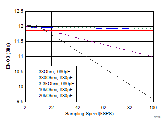
The following figure provides the ENOB achieved from the ADS7056 at different throughout with different input impedances. Note that all the results for the following graph were taken with a 100-Hz analog input signal and without an ADC driver amplifier.

Design Featured Devices
| Device | Key Features | Link | Similar Devices |
|---|---|---|---|
| ADS7040 | 8-bit resolution, SPI, 1-Msps sample rate, single-ended input, AVDD/Vref input range 1.6V to 3.6V. | Ultra-low-power, ultra-small-size SAR ADC, 8-bit, 1MSPS, single ended | Analog-to-digital converters (ADCs) |
| ADS7041 | 10-bit resolution, SPI, 1Msps sample rate, single-ended input, AVDD/Vref input range 1.6V to 3.6V. | Ultra-low power and ultra-small size SAR ADC, 10-bit, 1 MSPS, single ended | |
| ADS7042 | 12-bit resolution, SPI, 1-Msps sample rate, single-ended input, AVDD/Vref input range 1.6V to 3.6V. | 12-Bit, 1MSPS, Ultra-Low-Power, Ultra-Small-Size SAR ADC With SPI | |
| ADS7056 | 14-bit resolution, SPI, 2.5-Msps sample rate, single-ended input, AVDD/Vref input range 1.6V to 3.6V. | 14-bit 2.5-MSPS ultra-low-power ultra-small-size SAR ADC with SPI |
The ADS7042 and ADS7056 use the AVDD as the reference input. A high-PSRR LDO, such as the TPS7A47, should be used as the power supply.
Link to Key file
Texas Instruments, source files for SBAA256, SBAC178 support files