Single-Ended to Differential Signal Conversion Using an Op Amp and FDA for Unipolar Signals
| Input | ADC Input | Digital Output ADS7057 |
|---|---|---|
| Vin Min = –3.3V | AINP = 0V AINM = 3.3V |
2000H 819210 |
| Vin Max = 3.3V | AINP = 3.3V AINM = 0V |
1FFFH 819110 |
| AVDD | GND | DVDD |
|---|---|---|
| 3.3V | 0V | 1.8V |
Design Description
This design is intended to demonstrate how to convert a unipolar, single-ended signal into a unipolar, fully-differential signal and drive a differential ADC (for more information on these and other signal types, please refer to the TI Precision Labs training titled SAR ADC Input Types). Compared to a single-ended device, a fully-differential ADC has twice the dynamic range which improves the AC performance of the converter. Many common systems, for example Sonar Receivers, Flow Meters, and Motor Controls, benefit from the higher performance of a differential ADC. The equations and explanation of component selection in this design can be customized based on system specifications and needs. For more information on a similar design using a bipolar input, see the cookbook circuit titled Single-Ended to Differential Using an Op Amp and FDA for Bipolar Signals.
Specifications
| Specification | Calculated | Simulated |
|---|---|---|
| Transient ADC Input Settling (at 250ksps) | < 0.5 × LSB = 201µV | 144.8µV |
| Conditioned Signal Range (at 250ksps) | > 99% ADC FSR = > 6.53V | 6.60V |
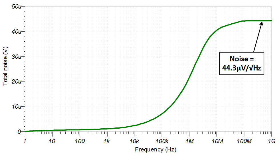
| Noise | 43.8µV ÷ √Hz | 44.3µV ÷ √Hz |
Design Notes
- The ADS7057 was selected because of its throughput (2.5Msps), size (2.25mm²), and low-latency (successive approximation register, or SAR, architecture).
- Determine the linear range of the fully-differential amplifier (ADC driver) based on common mode, output swing, and linear open-loop gain specification. This is covered in the component selection section.
- Determine the linear range of the op amp (signal conditioning) based on common mode, output swing, and linear open-loop gain specification. This is covered in the component selection section.
- Select COG (NPO) capacitors for Cfilt, to minimize distortion.
- For best performance, consider using a 0.1% 20ppm/°C film resistor, or better, to minimize distortion.
- The TI Precision Labs - ADCs training video series covers methods for selecting the charge bucket circuit Rfiltx and Cfilt. These component values are dependent on the amplifier bandwidth, data converter sampling rate, and data converter design. The values shown here will give good settling and AC performance for the amplifier and data converter in this example. If you modify the design you will need to select a different RC filter. Refer to Introduction to SAR ADC Front-end Component Selection for an explanation of how to select the RC filter for best settling and AC performance.
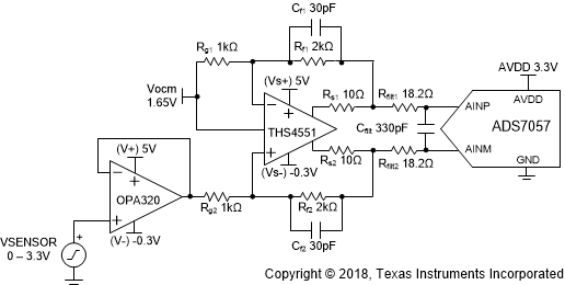
Component Selection
- Select a fully-differential
amplifier capable of driving the ADC:
THS4551 – Low noise, precision, 150MHz, fully-differential amplifier- Wide input common-mode voltage:
- Linear output (requirement:
0V to 3.3V at each output):
- Wide input common-mode voltage:
- Select a wide bandwidth operational
amplifier:
OPA320 – Precision, zero-crossover, 20MHz, RRIO, operational amplifier- Gain bandwidth product >12.5MHz (>5 times the sampling rate)
- Input common-mode voltage (requirement: 0 - 3.3V):
- Linear output:
- Combined worst-case linear
range (calculated from supplies used with OPA320):
Note:The operational amplifier is used to protect the sensor from any charge kickbacks that occur when the ADC connects or disconnects the sampling capacitor. This amplifier may not be needed if the sensor has a high-output impedance. A negative rail is used for both the OPA320 and THS4551 based on the assumption that the sensor is operating with a negative rail; this also provides the highest performance from the ADC by providing the full scale input range.
- Select Rfx and
Rgx
- The combination of Rfx and Rgx sets the gain of the system. With an input range of 0V - 3.3V and an ADC full scale of ±3.3V, a gain of 2 was selected for this system.
- The values of Rfx = 2k and Rgx = 1k were selected to both provide the desired gain as well as limit the current through the feedback network, thus minimizing power consumption of the system.
- Select Rsx
- It is important to connect small resistors at the output of the amplifier, in this case 10Ω, to flatten the output impedance and improve stability of the system.
- Select Rfiltx and Cfilt values for
settling of 250-kHz input signal and sample rate of 2.5Msps:
- Refine the Rfilt and Cfilt Values is a Precision Labs Video showing the methodology for selecting Rfiltx and Cfilt. The final value of 18.2Ω and 330pF proved to settle to well below ½ of a least significant bit (LSB) within the acquisition window.
DC Transfer Characteristics
The following graph shows the simulated output for a 0 - 3.3V input. The analog front end has a linear output of ±3.3V which matches the full-scale range (FSR) of the ADC (with AVDD = 3.3V).

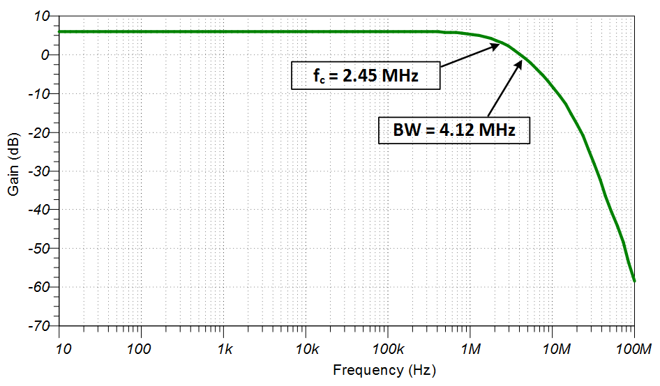
AC Transfer Characteristics
The bandwidth of the analog front end is simulated to be 4.12MHz at the gain of 0dB which is a linear gain of 1. This bandwidth allows the inputs of the ADC to adequately settle for a 250-ksps input signal.
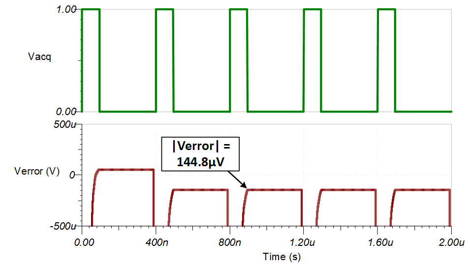
Transient ADC Input Settling Simulation
The following simulation shows the ADC sample and hold capacitor settling for a 3.3-V DC input signal. This simulation shows that the analog front end is able to drive the ADC with a large step input (from 0V to 3.3V) so it settles to within ½ of an LSB (approximately 200µV) in the allotted acquisition time (95ns). Refer to Introduction to SAR ADC Front-End Component Selection for detailed theory on this subject, and follow the link at the end of this design to download these simulation files.
Noise Simulation
This section walks through a simplified noise calculation, providing a rough estimate to compare with the simulated result. The resistor noise is included in this calculation as it is a significant portion of the overall noise of the system. Note that the resistor noise can be reduced by using smaller value resistors, but at the expense of increased power consumption through the feedback network.
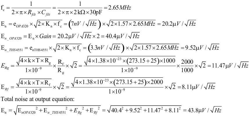
Note that calculated and simulated match well. Refer to the TI Precision Labs - ADCs training video series for detailed theory on this subject.
Design Featured Devices
| Device | Key Features | Link | Similar Devices |
|---|---|---|---|
| ADS7057 | 14 bit, 2.5 Msps, fully-differential input, SPI, 2.25mm2 package | 14-Bit, 2.5MSPS, Differential Input, Small-Size Low-Power SAR ADC | Precision ADCs |
| THS4551 | 150MHz, 3.3nV/√Hz input voltage noise, fully-differential amplifier | Low Noise, Precision, 150MHz, Fully Differential Amplifier | Fully differential amplifiers |
| OPA320 | Precision, zero-crossover, 20MHz, 0.9pA Ib, RRIO, operational amplifier | Precision, zero-crossover, 20MHz, 0.9pA Ib, RRIO, CMOS operational amplifier | Operational amplifiers (op amps) |
The ADS7057 uses the AVDD as the reference input. Use a high-PSRR LDO, such as the TPS7A47, as the power supply.
Link to Key files (TINA):
Texas Instruments, design files for SBAA264, SBAC188 software support
Revision History
Changes from Revision A (March 2019) to Revision B (September 2024)
- Updated the format for tables, figures, and cross-references throughout the documentGo
Changes from Revision * (January 2018) to Revision A (March 2019)
- Downstyle the title and changed title role to 'Data Converters'. Added link to circuit cookbook landing page.Go