SBAA266B February 2018 – September 2024 ADC122S021 , ADC122S051 , ADC122S051Q-Q1 , ADC122S101 , LM35 , LMP7715 , LMP7721
| Input | ADC Input | Digital Output ADC122S021 |
|---|---|---|
| VinMin = 0.03V | IN1 = 0.14 | 115 = 0x073 |
| VinMax = 1.07V | IN1 = 4.88 | 3998 = 0xF9E |
| VinMin = 0V | IN2 = 0V | 0 = 0x000 |
| VinMax = 1V | IN2 = 1V | 819 = 0x333 |
| Power Supplies | ||
|---|---|---|
| V+, VA | V– | |
| 5V | 0V | |
Design Description
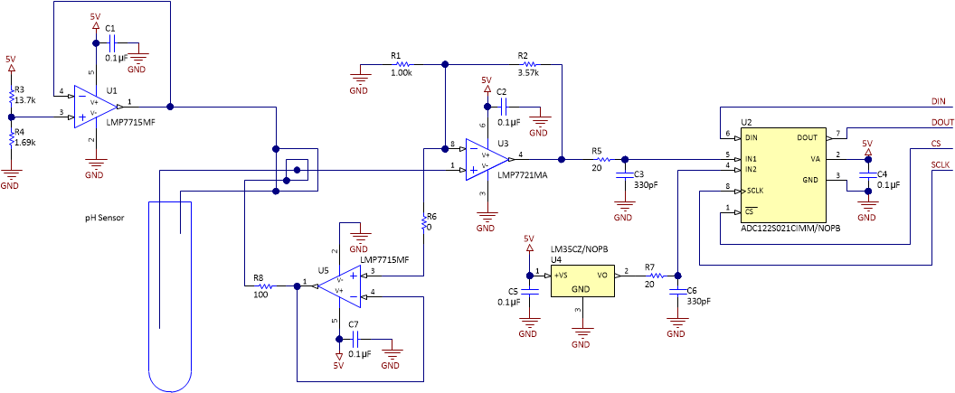
This design shows a low Ibias amplifier being used to drive a SAR ADC. A sensor with high output impedance requires an amplifier with a low input bias current to minimize errors. Examples of applications where this type of sensor can be used include gas detectors, blood gas analyzers, and air quality detectors. In this design, a pH probe is used for the sensor. The output impedance of a pH probe can be from 10MΩ to 1000MΩ. If a pH probe is used that has an output impedance of 10MΩ with an op amp that has 3nA of input bias current, then the error is due to the input bias current of the op amp is 30mV. Using the input signal amplitude and gain described in the component selection section, this 30mV equates to an error of about 2.9%. If an op amp with an input bias current of 3fA is used, the error is decreased to 30nV.
The output of the pH sensor does not quickly change, so a lower speed ADC can be used. The value from the pH sensor changes as the temperature changes so a two channel ADC was selected so that one channel can be used to monitor the temperature. The ADC122S021 used in this design is a 2-channel, 12-bit, ADC that can sample up to 200ksps.

Specifications
| Specification | Calculated | Simulated | Measured |
|---|---|---|---|
| Ibias | 20fA | 118fA | 20fA |
Design Notes
- Use COG (NPO) capacitors for C3 and C6.
- Each IC needs to have a bypass capacitor of 0.1μF.
- PCB layout is very important. See the LMP7721 Multi-Function Evaluation Board Users’ Guide.
- The PCB must be clean. See the LMP7721 Multi-Function Evaluation Board Users’ Guide.
- For more information on low leakage design, see Design femtoampere circuits with low leakage.
Component Selection
- The output voltage of a pH sensor
changes as the temperature changes. At 0°C, the output voltage outputs
54.2mV/pH, at 25°C, the output voltage outputs 59.16mV/pH, and at 100°C, the
output voltage outputs 74.04mV/pH. This means that the maximum swing of the pH
sensor around the bias point of the pH sensor is ±518.3mV at 100°C. The maximum
output of the LMP7721 needs to be limited to ±2.4V to allow for headroom. That
sets the gain of the LMP7721 at:
2.4V / 0.5183V = 4.6V/V
Setting resistors R2 = 3.57kΩ and R1 = 1kΩ, sets this gain. - Since the input of the LMP7721
must be from 0V to 5V, the pH sensor needs to be biased above ground. Resistors
R3 = 13.7kΩ and R4 = 1.69kΩ in a voltage divider configuration sets the input of
U1 to:
5V · 1.69kΩ / (1.69kΩ + 13.7kΩ) = 549mV
U1 has a gain of 1V/V so the bias of the pH sensor is also at 549mV. Since the pH sensor can swing –518.3mV below the bias point, this keeps the input of the LMP7721 above ground. The output of the LMP7721 is centered at:
0.549V · 4.6V/V = 2.52V
and can swing ±2.4V above and below the center point. - U5 is used to set the voltage of the guard ring and is set with a gain of 1V/V and the input is the signal on the –IN pin of the LMP7721.
- The output of the LMP7721 is connected to one of the inputs of the ADC122S021 SAR ADC. The sampling capacitor of the ADC is 33pF and the external capacitor placed next to the pin of the ADC must be 10 times larger, or 330pF. A small resistor of 20Ω is added in series to isolate the capacitor from the LMP7721.
- Because the output of the pH sensor changes as the temperature changes the LM35, a temperature sensor, is connected to channel 2 of the ADC122S021. A 330pF capacitor along with a 20Ω series resistor is used on the output of the temperature sensor.
DC Transfer Characteristics
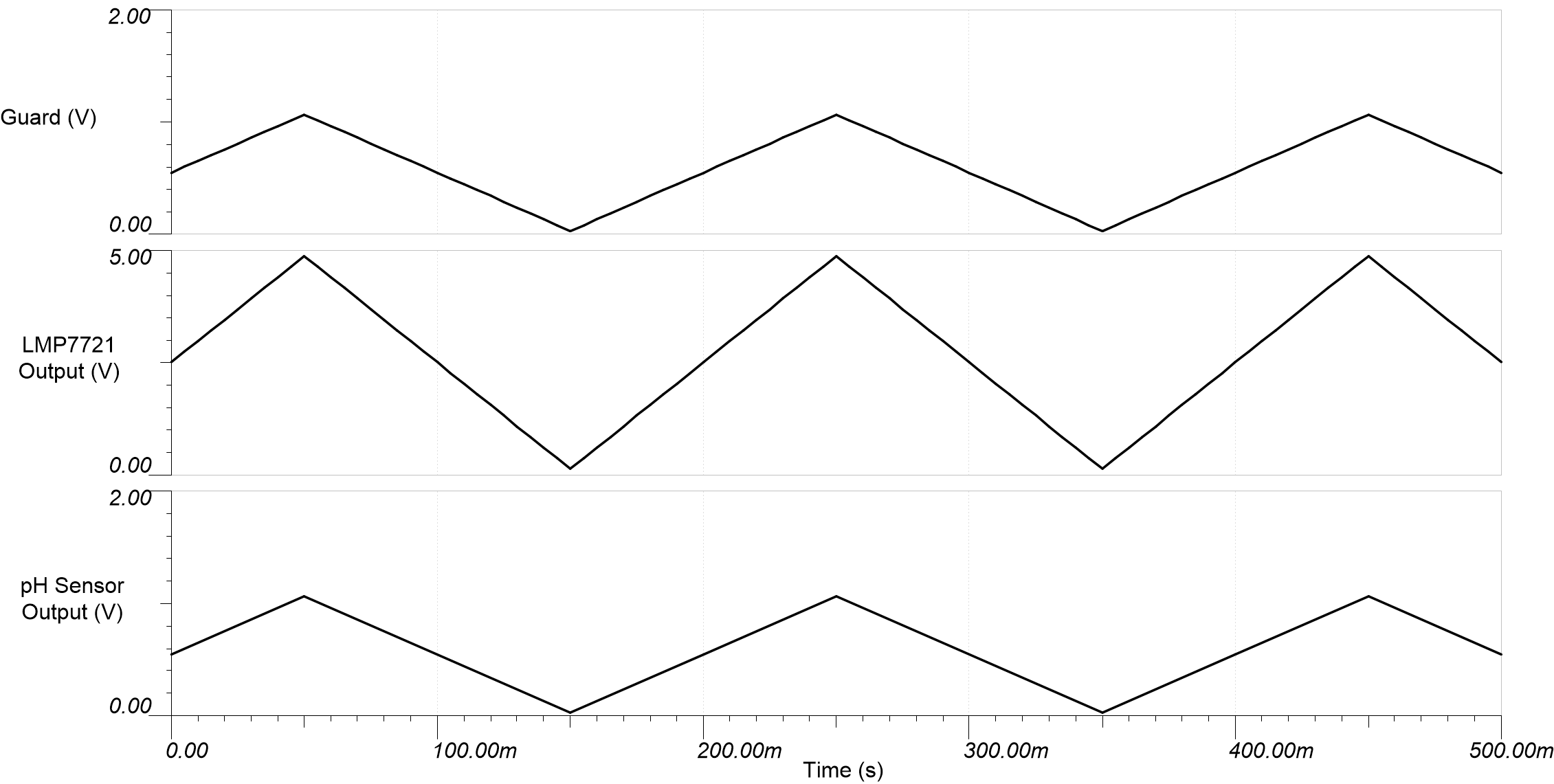
The following graph shows the pH sensor input to the LMP7721, the Guard voltage, and the LMP7721 output. This data is for 100°C, when the pH sensor output has the largest possible output swing.

Layout
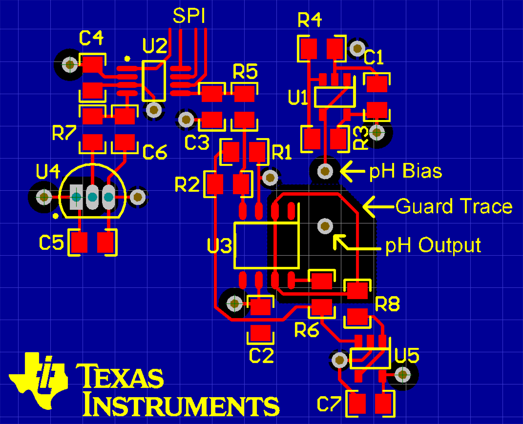
The PCB layout is very important for a low Ibias circuit. Current leakage occurs between two traces when there a voltage potential between the traces. This is the reason for the guard trace. The guard trace is set to a voltage close to the input voltage to minimize the leakage between the input of the LMP7721 and the outside world. The LMP7721 includes two unused pins (pins 2 and 7) that can be used to simplify the layout of a guard trace.
The following image shows a sample layout. The output of the pH sensor and the +IN input of the LMP7721 are separated from the rest of the circuit by the guard trace, which is close to the input voltage. This minimizes the leakage on the input of the LMP7721. The bias of the pH sensor is located outside of the guard. Leakage between the bias point and the rest of the circuit is not important. Solder mask must not cover the area inside the guard trace. If there is a ground plane on the bottom side of the board or other internal planes, then the planes need to have a keep out area underneath the guard area.

Design Featured Devices
| Device | Key Features | Link | Similar Devices |
|---|---|---|---|
| ADC122S021 | 12 bit, SPI, 2 channel, 50ksps to 200ksps, single ended input | www.ti.com/product/adc122s021 | www.ti.com/adcs |
| LMP7721 | Ultra-low input bias current of 3fA, with a specified limit of ±20fA at 25°C, offset voltage ±26µV, GBW 17MHz | www.ti.com/product/lmp7721 | www.ti.com/opamps |
| LMP7715 | Input offset voltage ±150µV, input bias current 100fA, input voltage noise 5.8nV/√Hz, gain bandwidth product 17MHz | www.ti.com/product/lmp7715 | www.ti.com/opamps |
| LM35 | Calibrated directly in degrees Celsius, Linear + 10mV/°C scale factor, 0.5°C verified accuracy (at 25°C), rated for full –55°C to 150°C range | www.ti.com/product/lm35 | www.ti.com/temperature |
Design References
See Analog Engineer's Circuit Cookbooks for TI's comprehensive circuit library.