SBAA269B February 2018 – September 2024 ADS8689 , ISO7741
| Input | ADC Input | Digital Output ADS7042 |
|---|---|---|
| VinMin = –12.288V | AIN_P = –12.288V, AIN_N = 0V | 8000H or -3276810 |
| VinMax = 12.288V | AIN_P = 12.288V, AIN_N = 0V | 7FFFH or 3276710 |
| Power Supplies | ||
|---|---|---|
| AVDD | Vee | Vdd |
| 5V | 6.5V | 5V |
Design Description
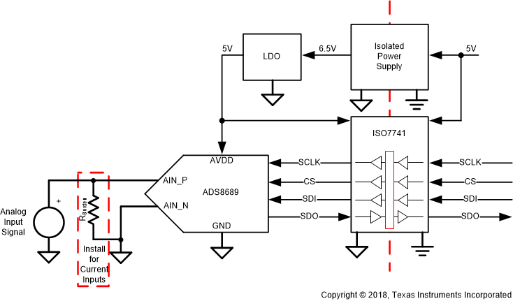
This design shows a digitally isolated high-voltage SAR ADC that is capable of full AC performance at maximum throughput. This design is intended for channel-to-channel isolated analog input modules as well as measuring a signal with a very large common mode. Programmable logic controller, analog input modules, and many 4- to 20-mA signal applications benefit from this design. See Isolated Power Supply Low-Noise, 5V, 100mA for details on the isolated power supply design for these applications. This cookbook includes links to design files.
This circuit implementation is applicable in applications such as Analog Input Modules, Electrocardiogram (ECG), Pulse Oximeter, and Bedside Patient Monitors.

Specifications
| Specification | Calculated | Measured |
|---|---|---|
| SCLK Frequency | 6.66MHz | 6.67MHz |
| Sampling Rate | 100ksps | 100ksps |
| Signal-to-Noise Ratio (SNR) | 92dB | Min: 92.29dB Max: 92.46dB |
| Total Harmonic Distortion (THD) | –112dB | Min: –108.8dB Max: –111.38dB |
Design Notes
- Select a SAR ADC that meets the input voltage range, sampling rate, and resolution for the system. This is covered in the component selection section.
- Select a digital isolator that allows for the required isolation specification as well as the correct number of channels and channel directions. This is covered in the component selection section.
- Install the burden resistor for current inputs. This design removes any common mode limitation of the inputs due to the channel-to-channel isolation. Select the burden resistor so that the maximum current input stays within the full scale range of the SAR ADC.
Component Selection
- Select a SAR ADC that meets the
input voltage range, sampling rate, and resolution for the system:
- Desired input range: ±12V
- Desired effective number of bits (ENOB): 14 bits
- Desired sampling rate: 100ksps
- ADS8689 input range: ±12.228V
- ADS8689 ENOB: 14.8 bits
- ADS8689 maximum sampling
rate: 100ksps Note:
There is a wide selection of TI SAR ADCs that match the specifications in the previous list.
- Select a digital isolator that
allows for the required isolation specification as well as the correct number of
bidirectional channels:
- TI offers digital isolators with isolation rating ranging from 2.5kVRMS to 5.7kVRMS.
- Choose isolation ratings based on the system requirements.
- For a standard SPI interface, the digital isolator needs to be 4-channels with 3 channels in the same direction and 1 channel in the opposite direction.
- The ISO774x is a digital isolator family for 4-channel devices with all combinations of channel directions and the ability to select a 2.5kVRMS or a 5.0kVRMS isolation rating.
- Understand the expected delays to
the digital signal from the digital isolator:
- The ISO7741 has a typical propagation delay of 10.7ns with a maximum of 16ns.
- Round trip isolation delay is 21.4ns typical or 32ns maximum.
- SCLK is running at 6.66MHz resulting in a period of 150ns.
- The typical round trip delay is 14% of the SCLK period.
- The maximum round trip delay is 21% of the SCLK period.
Note:The delay from the isolator results in a delay between the optimal SDO read relative to SCLK and the actual SDO read. This delay can be adjusted for by adding an SCLK return signal that travels through the digital isolator to all for the SDO to be read at exactly the correct time. Adding a return clock requires another channel of isolation.
Measured FFT
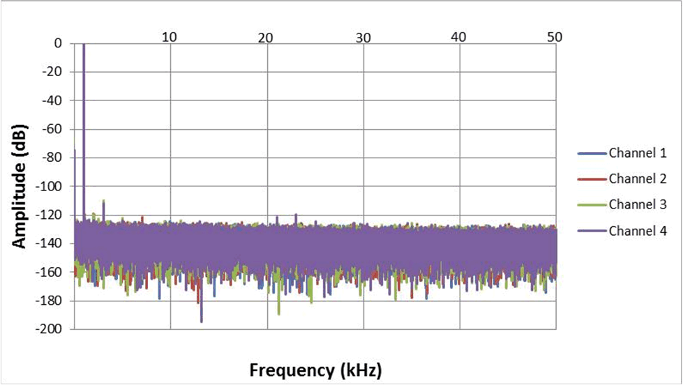
This performance was measured on a custom 4-channel, channel-to-channel isolated ADS8689 PCB. The input signal is a 24Vpp, 1-kHz sine wave. The AC performance indicates minimum SNR = 92.2dB and minimum THD = –108.8dB, which matches well with the specified performance of the ADC of SNR = 92dB and THD = –112dB.
| Channel | SNR(dB) | THD (dB) |
|---|---|---|
| 1 | 92.29 | –109.95 |
| 2 | 92.38 | –108.82 |
| 3 | 92.46 | –109.53 |
| 4 | 92.42 | –111.38 |

TVS Diode Performance Degradation
A 14-V bidirectional TVS diode was used in this design to protect the input of the SAR ADC. The TVS diode actually degrades total harmonic distortion (THD) due to the added capacitance. The THD was seen to be around 6dB worse with the TVS diode installed versus uninstalled.
Design Featured Devices
| Device | Key Features | Link | Similar Devices |
|---|---|---|---|
| ADS8689(1) | 16 bit resolution, SPI, 100-ksps sample rate, single-ended input, and ±12.288-V input range. | 16-Bit, 100-kSPS, 1-Ch SAR ADC with programmable (±12/±10/±6/±5/±2.5V) input ranges on +5V supply | Precision ADCs |
| ISO7741(2) | High-speed, robust-EMC reinforced quad-channel digital isolator | Robust EMC, quad-channel, 3/1, reinforced digital isolator | Isolation |
Link to Key Files
Texas Instruments, Source files for SBAA269, software support.