SBAA282B March 2018 – September 2024 ADS8319 , OPA365
| Input | ADC Input | Digital Output ADS8319 |
|---|---|---|
| Vin Min = 0.1V | Vadc_in = 4.9V | FAE1H or 6422510 |
| VinMax = VREF = 4.9V | Vadc_in = 0.1V | 051FH or 131110 |
| Vcc | Vee | Vcm | VREF | AVDD | DVDD |
|---|---|---|---|---|---|
| 5.3V | GND (0V) | 2.5V | 5V | 5V | 5V |
Design Description
This cookbook is intended to demonstrate a method of designing an antialiasing filter for a single-ended SAR ADC input using the Antialias Filter Designer on TI’s Analog Engineer’s Calculator. The objective of the tool is to find filter specifications that attenuates alias signals to one-half LSB of a given ADC. This design approach uses a fixed cutoff frequency and the example circuit uses the ADS8319 ADC. This single-ended device circuit is practical for low-power applications such as data acquisition, lab instrumentation, oscilloscopes and digitizers, analog input modules, and battery-powered equipment.
| Specification | Calculated / Goal | Simulated |
|---|---|---|
| Attenuate 1mV alias signal at Nyquist to ½ LSB Vin_Nyquist = 1mV at 250kHz |
Vout_Nyquist <= ½ LSB ½ LSB = 38.14µV at 250kHz |
Vout_Nyquist = 21µV Attenuation = –33.43dB |
| Transient ADC Input Settling | < 0.5 LSB or 38.15µV | 91.5nV |
| Noise | 78.9µV | 87.77µV |
| Bandwidth | 50kHz | 50.1kHz |
Design Notes
- TI Precision Labs introduces the concept of frequency domain aliasing and describes how aliases are error sources to avoid or minimize. The video on Aliasing and Anti-aliasing Filters covers how an antialiasing filter can be used to minimize these aliasing errors.
- The active filter in this cookbook is designed using TI’s Analog Engineer’s Calculator and TI FilterPro. This software can be used to design active filter circuits for many applications.
- Use 0.1%–1% tolerance resistors and 5% tolerance capacitors or better for good system accuracy.
- RC charge bucket circuits are specially designed for each system; TI’s Precision Labs video on Refining Rfilt and Cfilt Values explains how to optimize the RC charge bucket.
- Circuit simulations are modeled with schematics and diagrams made using TINA-TI simulation software.
- For detail on choosing the right driver op amp, building and simulating the ADC model, and finding the RC charge bucket values, see the TI Precision Labs video series Introduction to SAR ADC Front-End Component Selection.
Component Selection
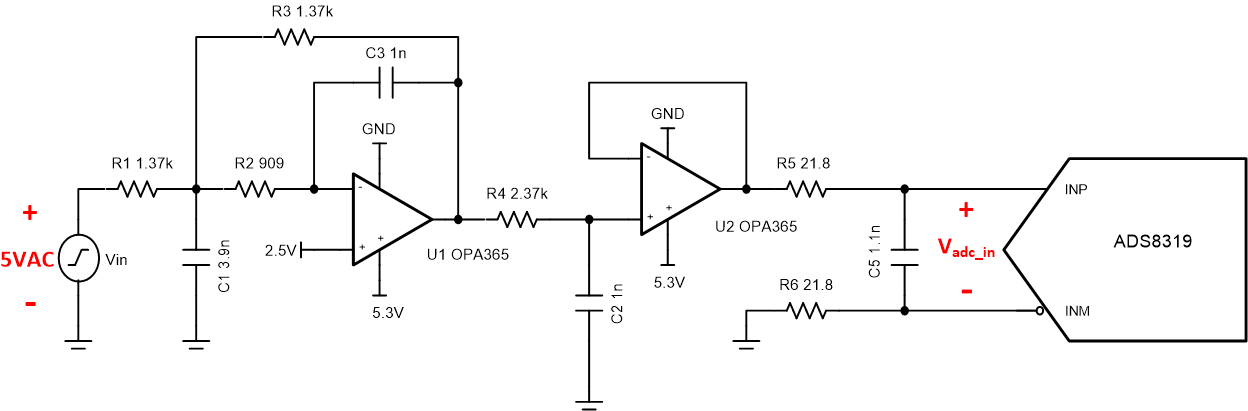
- Once a single-ended ADC has been chosen, determine whether the antialias filter is designed with a set cutoff frequency or set filter order. If the frequency is set, continue through the following steps. If the filter order is set, use the "Find Usable Frequency Range" tab in the Analog Engineer's Calculator. Both methods use tools from the Analog Engineer’s Calculator.
- Using the Find Filter Order tab of the Anti-Alias Filter Designer, choose between a Bessel and Butterworth filter under Choose Filter Type. Bessel is chosen in this case for maximum flatness in the pass band and linear phase response.
- Fill in the Nyquist Frequency to be ½ of the sampling rate of the ADC. The ADS8319 has a sampling rate of 500ksps so the Nyquist frequency is 250kHz.
- Determine the desired cutoff frequency of the filter to be designed and enter it in the Cutoff Frequency box; a general guideline is for the cutoff frequency to be one decade above the desired input frequency. In this case, the input frequency is 5kHz so the cutoff frequency is set to 50kHz.
- For the Alias Signal Amplitude at Nyquist Frequency field, enter the largest expected alias signal amplitude that attenuate to ½ LSB at the Nyquist frequency. This number ranges from microvolts up to full scale voltage. In this low-noise system, a maximum alias signal amplitude of 1mVpp is expected.
- The Full Scale Range of the ADC is typically equal to Vref and is set to 5V in this system. The bit resolution of the ADS8319 is 16 bits and is filled into Number of Bits.
- After clicking OK, the results displayed on the right side of the calculator are used to design the necessary antialias filter.
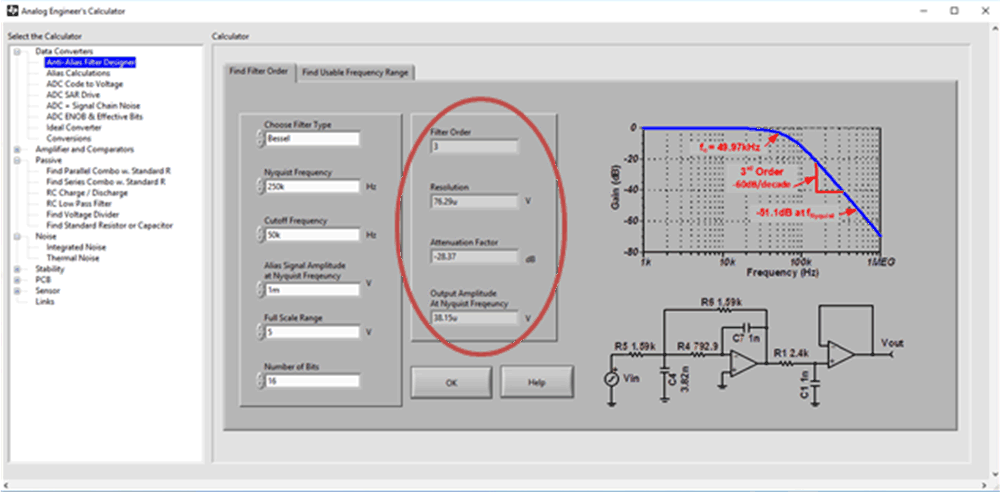
With the resulting filter specifications, the lowpass antialias filter can be designed by transcribing these numbers into TI FilterPro. The circuit specifications in this cookbook are fnyquist = 250k, fc = 50k, Valias = 1mV, FSR = 5V, and N bits = 16, so the Bessel example from Design Approach 1 is used continuing.
On startup, TI FilterPro asks for the filter specifications to design around. After the final screen, an active filter circuit is displayed, and this is the antialias filter of the system. Refer to the following screenshots for the steps using FilterPro.
In step 1, Lowpass is selected since an antialias filter is a specific lowpass filter.
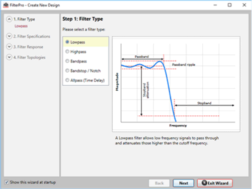
In step 2, the values for Pass-band Frequency (fc) and filter order are filled in from the Analog Engineer’s Calculator. The option to Set Fixed filter order must be selected to match calculated parameters.
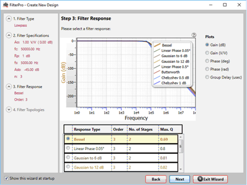
For step 3, select the filter type to match calculations; Bessel is chosen in this example for maximum flatness in the pass band and linear phase response.
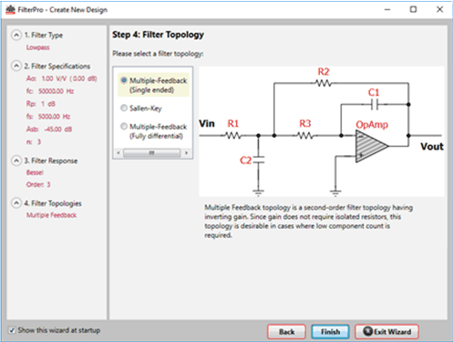
Multiple feedback topology is chosen in step 4 because the filter attenuation is not limited by the bandwidth of the op amp. This topology has the disadvantages of inverting a signal and offering low input impedance. Sallen-Key can also be selected since it is a non-inverting topology with high-input impedance, but at higher frequencies the attenuation of the filter converges or even rises due to the bandwidth limitations of the op amp.
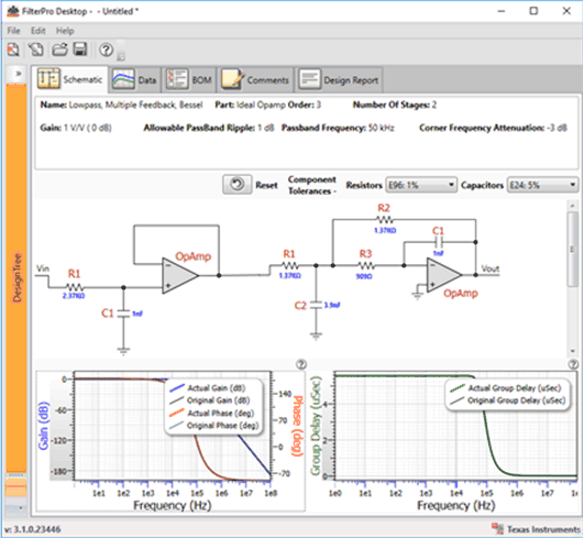
After clicking Finish, the filter schematic is displayed along with performance specifications of the resulting filter. Component tolerances can be adjusted using the right side drop-down menus; 1% resistors and 5% capacitors are chosen here as practical considerations. Component values can be modified by clicking on a number and entering new values.
The circuit previously pictured can be designed in TINA-TI for simulation. Performance characteristics are documented in the following sections.
DC Transfer Characteristics
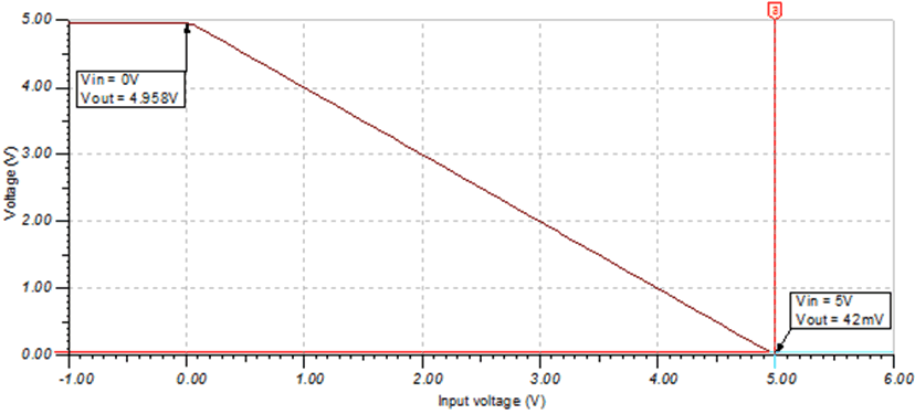
The following graph shows a linear output response for filter inputs from 0V to 5V. Since the filter amplifier is in inverting configuration, the output voltage is a function of Vout = –Vin + 5V.
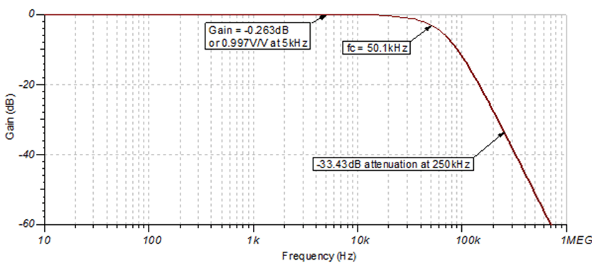
AC Transfer Characteristics
The bandwidth is simulated to be 50.1kHz, about 100Hz away from the desired value entered in the Analog Engineer’s Calculator. At the Nyquist frequency, signals are attenuated by –33.43dB, which would lower the amplitude of the input alias signal to 21.3µV. See the TI Precision Labs Op Amps: Bandwidth 1 for more details on this subject.
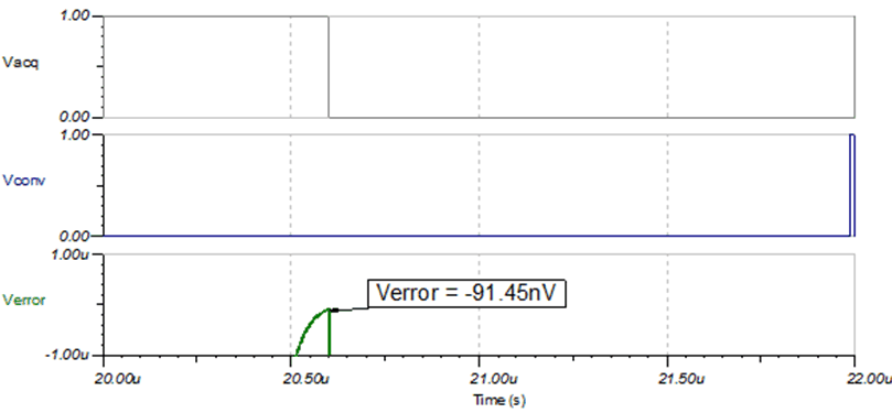
Transient ADC Input Settling Simulation
The following simulation shows the ADS8319 settling to a 5-Vpp AC signal at 5kHz through the data acquisition period. This type of simulation shows that the RC charge bucket components are properly selected. See the TI Precision Labs video on Refine the Rfilt and Cfilt Values for detailed theory on this subject.
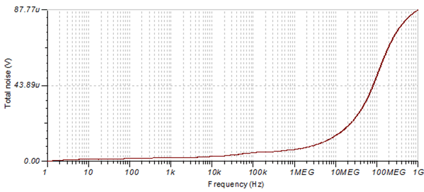
Noise Simulation
A simplified noise calculation is made here for a rough estimate. We neglect noise from the antialias filter in this calculation since it is attenuated for frequencies greater than 50kHz.

The value for enOPA365 is taken from a data sheet noise curve. Note that calculated and simulated noise values match well. Some of the discrepancy between the simulated and calculated noise is due to inaccuracy from the bandwidth of the OPA365 model. See TI Precision Labs video on Calculating the Total Noise for ADC Systems for detailed theory on noise calculations.
Design Featured Devices
| Device | Key Features | Link | Similar Devices |
|---|---|---|---|
| ADS8319 | 16-bit, 500kl, serial interface, micro-power, miniature, SAR ADC | Precision 16-Bit SAR Analog-to-Digital Converter (ADC) With SPI | Analog-to-digital converters (ADCs) |
| OPA365 | 50MHz, zero-crossover, low-distortion, high CMRR, RRI/O, single-supply operational amplifier | 2.2V, 50MHz, Low-Noise, Single-Supply Rail-to-Rail Operational Amplifier | Operational amplifiers (op amps) |
Link to Key Files
Texas Instruments, SBAC197 source files, support software