SBAA315B October 2018 – August 2024 ADS9224R , ADS9234R , THS4551 , TMUX1109
| Input (THS4551 Inputs) | ADC Input (THS4551 Output) | Digital Output ADS7042 |
|---|---|---|
| VinP = +0.23V, VinN = +3.866V, VinMin(Dif) = -3.636V | VoutP = +0.23V, VoutN = 3.866V, Vout(Dif) = -3.636V | 8E60H -2908810 |
| VinP = +3.866V, VinN =0.23V, VinMax(Dif) = +3.636V | VoutP = 3.866V, VoutN = +0.23V, Vout(Dif) = +3.636V | 71A0H +2908810 |
| Vcc | Vee | Vref | Vocm |
|---|---|---|---|
| 5 | 0V | 4.096V | 2.048V |
Design Description
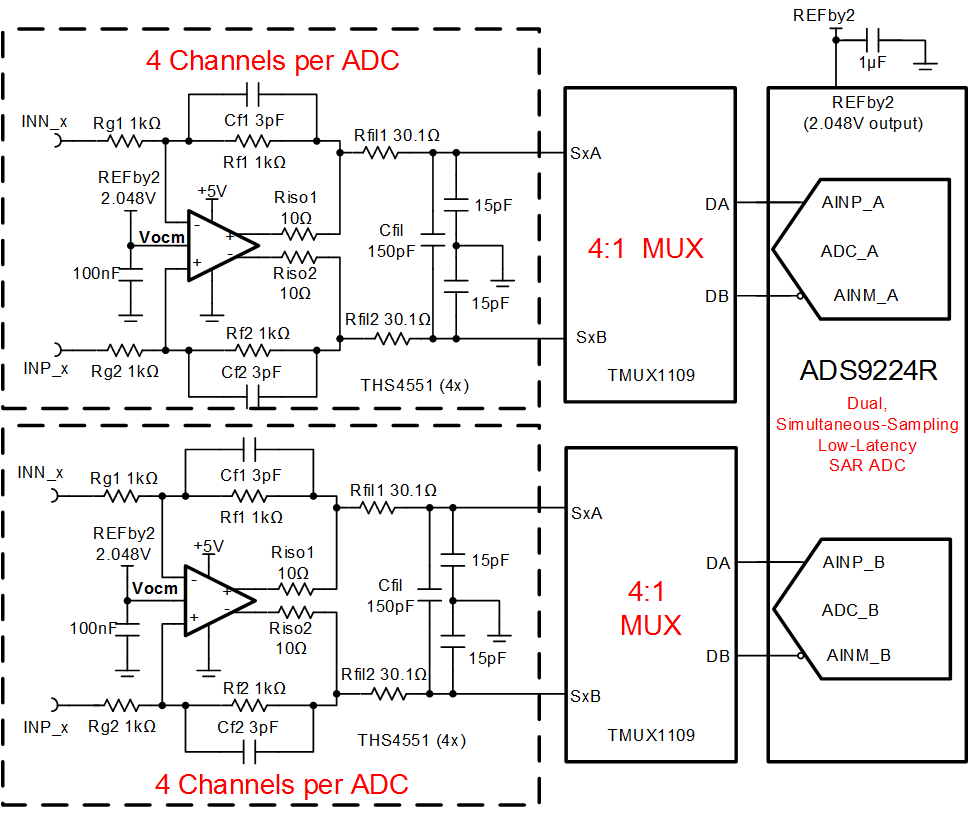
This dual simultaneous-sampling SAR ADC and 4 × 2 channel multiplexed analog front end data acquisition solution can measure differential voltage signals in the range of ±3.866V supporting ADC sampling rates up to 3-MSPS (or effective sampling rate of 750-kSPS per channel) with 16-B resolution. The circuit consists of a dual simultaneous sampling SAR ADC, with each SAR ADC connected to two 4:1 (2x) multiplexers, providing 4 differential input channels per ADC. Eight Fully Differential Amplifiers (FDAs) drive the multiplexed SAR ADC inputs. This circuit is applicable in the accurate measurement of dual simultaneous signals in applications such as Optical Modules and Analog Input Modules. It also can be used in motor drive applications such as Servo Drive Control Module, Servo Drive Position Feedback, and Servo Drive Position Sensor.
Specifications
| Specification | Goal | Calculated | Simulated |
|---|---|---|---|
| Dual ADC Sampling Speed | 3Msps | 3Msps | 3Msps |
| Sampling Rate per Channel (dual, simultaneous) | 750kSPS (3MSPS / 4) |
750kSPS (3-MSPS / 4) |
750-kSPS (3MSPS / 4) |
| Transient ADC Input Settling | << 1 LSB << 125µV |
NA | 20µV |
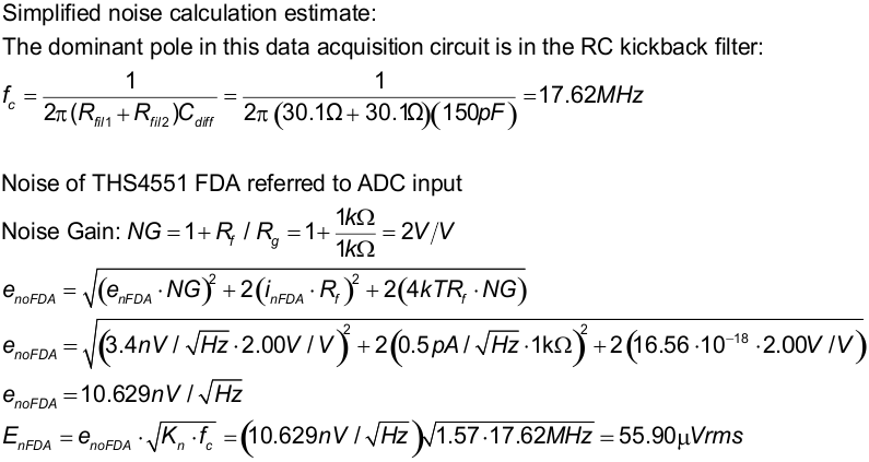
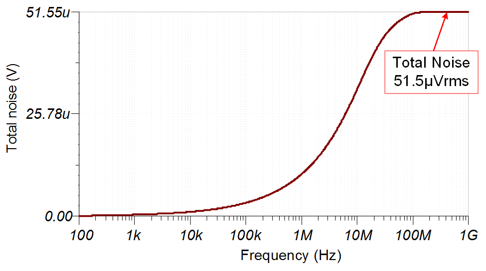
| Noise (at ADC Input) | 50µVrms | 55.9µVrms | 51.1µVrms |
Design Notes
- The ADS9224R was selected because of the dual simultaneous sampling and high throughput (3-MSPS) requirements.
- The TMUX1109 4:1 (2x) multiplexer was selected to support 4-channel differential inputs for each ADC.
- Find ADC full-scale range, resolution and common-mode range specifications. This is covered in the component selection.
- Determine the linear range of the FDA (THS4551) based on common-mode and output swing specification. This is covered in the component selection section.
- Select COG capacitors for all filter capacitors at the ADC input to minimize distortion.
- Select the FDA gain resistors RF1,2 , RG1,2. Use 0.1% 20ppm/°C film resistors or better for good accuracy, low gain drift and to minimize distortion.
- Introduction to SAR ADC Front-End Component Selection covers the methods for selecting the charge bucket circuit Rfil1, Rfil1 and Cfil. These component values are dependent on the amplifier bandwidth, data converter sampling rare, and data converter design. The values shown here will give good settling and AC performance for the amplifier and data converter in this example. If the design is modified, a different RC filter must be selected.
- The THS4551 is commonly used in high-speed precision fully differential SAR applications as it has sufficient bandwidth to settle to charge kickback transients from the ADC input sampling, and multiplexer charge injection and provides the common-mode level shifting to the voltage range of the SAR ADC.
Component Selection
Transient Settling Optimization
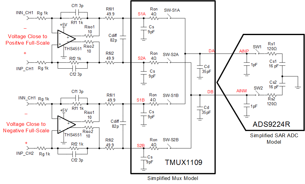
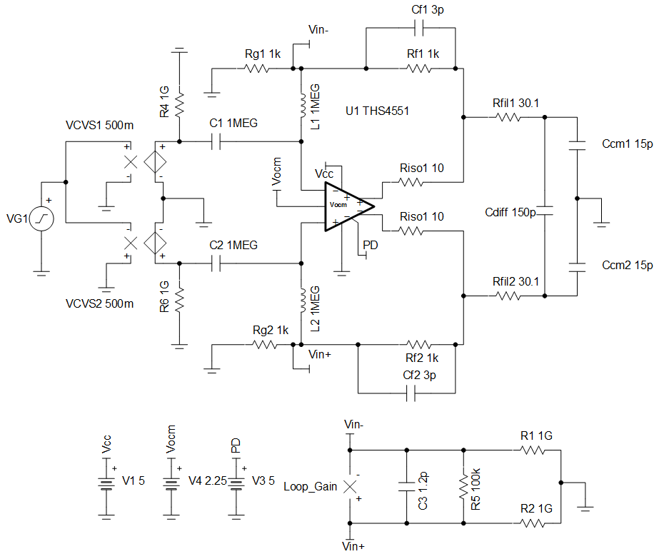
TINA simulation is used to optimize the RC kickback filter for stability and transient settling. The transient simulation incorporates two adjacent channels of the multiplexer (TMUX1109). To simulate worst case transient settling during the multiplexer scanning sequence, the two adjacent channels are set to a voltage close to positive full-scale and negative full-scale respectively. The multiplexer drain capacitance and series resistance are modeled in the multiplexer simulation circuit. The sample and hold capacitor of the SAR ADC must settle within the 16-bit resolution of the SAR ADC during the acquisition period. A simplified schematic of the simulation circuit follows:
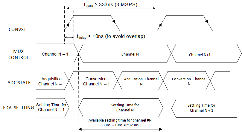
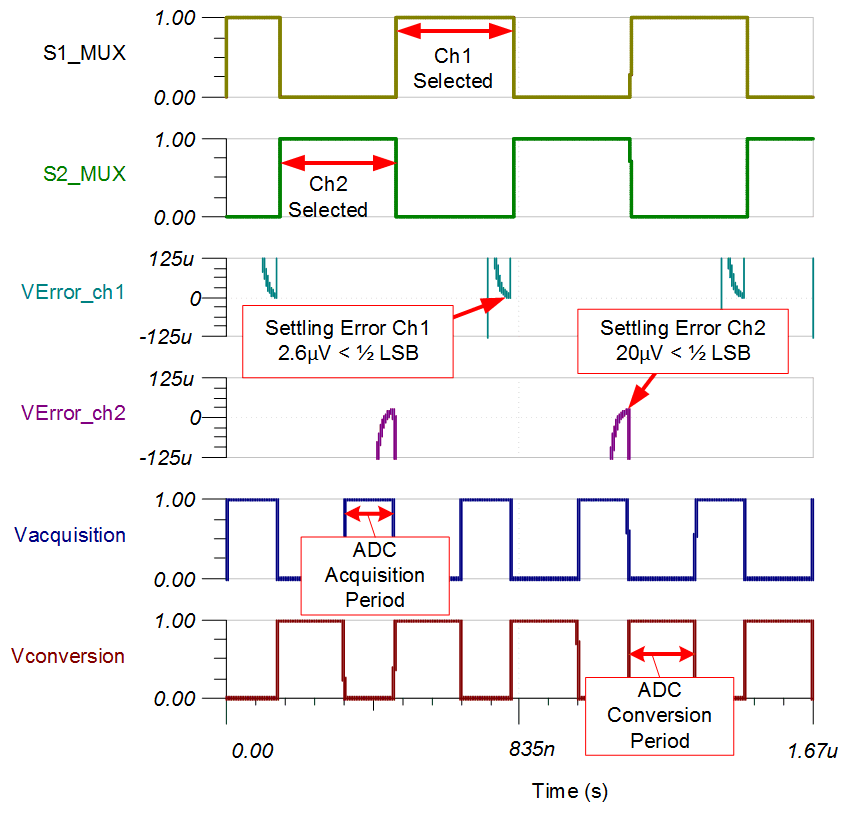
Multiplexer and ADC Control Timing
The following plot shows the ADC conversion control (CONVST) and multiplexer channel control timing. The ADS9224R supports a maximum sampling rate of 3Msps or a minimum cycle time of 333ns. To avoid switching channels prior to the rising edge of the CONVST signal, a small delay is implemented in the MUX channel control timing after the CONVST rising edge. Refer to TI design 16-Bit, 400-kSPS, Four-Channel MUX Data Acquisition System for High-Voltage Inputs Reference Design for detailed theory in the subject.
Transient Settling Results
The following TINA transient simulation shows settling of the FDA, multiplexer, and SAR ADC sample and hold after a full-scale step change between adjacent MUX channels. This type of simulation shows that the sample and hold kickback circuit, and AFE amplifier circuit is properly selected. See Introduction to SAR ADC Front-end Component Selection for an explanation of how to select the RC filter for best settling and AC performance.
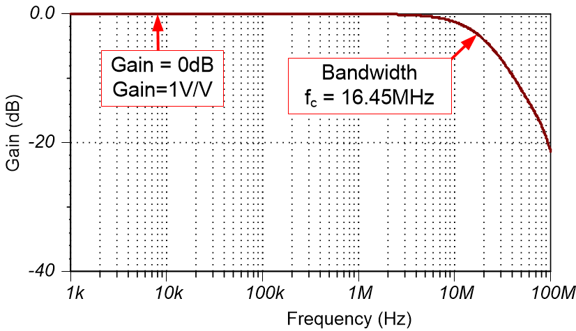
AC Transfer Characteristics
The circuit has a gain of 0-dB (1-V/V) and a simulated frequency bandwidth of 16.45-MHz. Notice that the calculated and simulated bandwidth compare well (calculated = 17.62MHz, simulated = 16.45MHz). See Op Amp Bandwidth for a general overview of bandwidth calculations and simulations.
The system bandwidth is set by the output filter:

Stability Simulation Graph
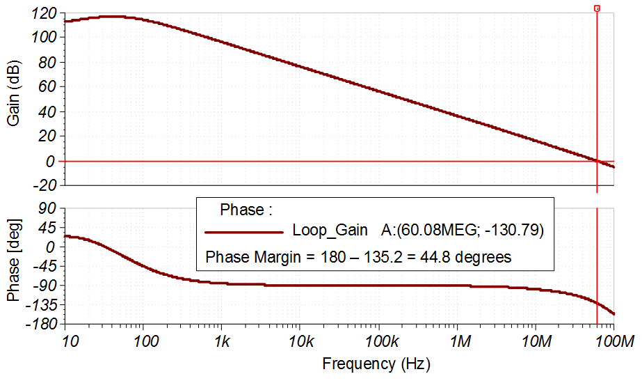
The following circuit is used in TINA to measure loop gain and verify phase margin using AC analysis in TINA. Resistors RISO = 10Ω are used inside the feedback loop to increase phase margin. The circuit has good stability (approximately 45 degrees of phase margin). See Op Amp Stability for detailed theory on this subject.
Noise Simulation
The following figure shows the TINA simulated total noise for the FDA circuit. See Calculating the Total Noise for ADC systems for detailed theory on this subject. Note that the calculated and simulated noise compare well (calculated = 55.9µVrms, simulated = 51.5µVrms).
Design Featured Devices
| Device | Key Features | Link | Other Possible Devices |
|---|---|---|---|
| ADS9224R | 16-bit resolution, SPI, 3-MSPS sample rate, fully-differential input, integrated 2.5-V reference, dual, simultaneous sampling, low-latency | 16-bit, 3MSPS, dual-channel, simultaneous-sampling SAR ADC with internal reference and enhanced SPI | Analog-to-digital converters (ADCs) |
| THS4551 | 150MHz, 3.3nV ÷ √ Hz input voltage noise, fully-differential amplifier | Low Noise, Precision, 150MHz, Fully Differential Amplifier | Fully differential amplifiers |
Link to Key Files
Texas Instruments, SBAC219 TINA files, software support