SBAA316A October 2018 – September 2024 ADS8528 , ADS8548 , ADS8568 , ADS8860 , INA826
| Input | ADC Input | Digital Output ADS7042 |
|---|---|---|
| –10V | –10V |
8000H |
| +10V | +10V | 7FFFH |
| AVDD | DVDD | Vref | Vcc | Vee |
|---|---|---|---|---|
| 5.0V | 3.0V | 5.0V | +15V | –15V |
Design Description
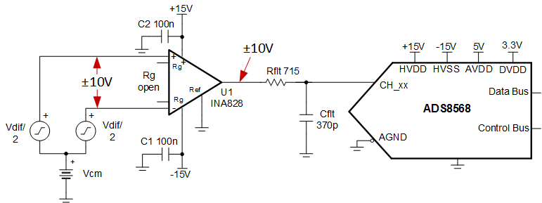
Instrumentation amplifiers are optimized for low noise, low offset, low drift, high CMRR and high accuracy. The INA828 instrumentation amplifier preforms a differential to single-ended conversion for a ±10-V range. The INA828 has excellent DC performance (that is, offset, drift), as well as good bandwidth. The ADS8568 is ideally suited to work with the INA828 as the ADC can be configured for a ±10-V single-ended input. To achieve the best settling, limit the sampling rate to 200kSPS or lower. For higher sampling rates see Driving High-Voltage SAR ADC with a Buffered Instrumentation Amplifier. Also, this design example uses unity gain (G=1) to translate a ±10-V differential input signal to a ±10-V single-ended output. For smaller input signals or higher gains, see Circuit for Driving an ADC with an Instrumentation Amplifier in High Gain. This circuit implementation is applicable to Industrial Transportation and Analog Input Modules that require precision signal-processing and data-conversion.
Specifications
| Specification | Goal | Calculated | Simulated |
|---|---|---|---|
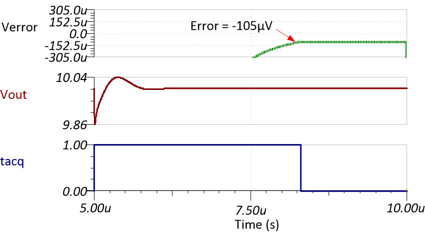
| Transient Settling Error | < 1/2 LSB (±152µV) | NA | –105µV |
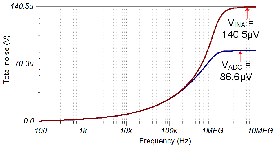
| Noise | < 20µV | 103µV | 86.6µV |
Design Notes
- The bandwidth of instrumentation amplifiers is typically not enough to drive SAR data converters at higher data rate. In this example, the sampling rate is reduced from 510kSPS to 200kSPS to achieve good settling. For full sampling rate see Driving High-Voltage SAR ADC with a Buffered Instrumentation Amplifier.
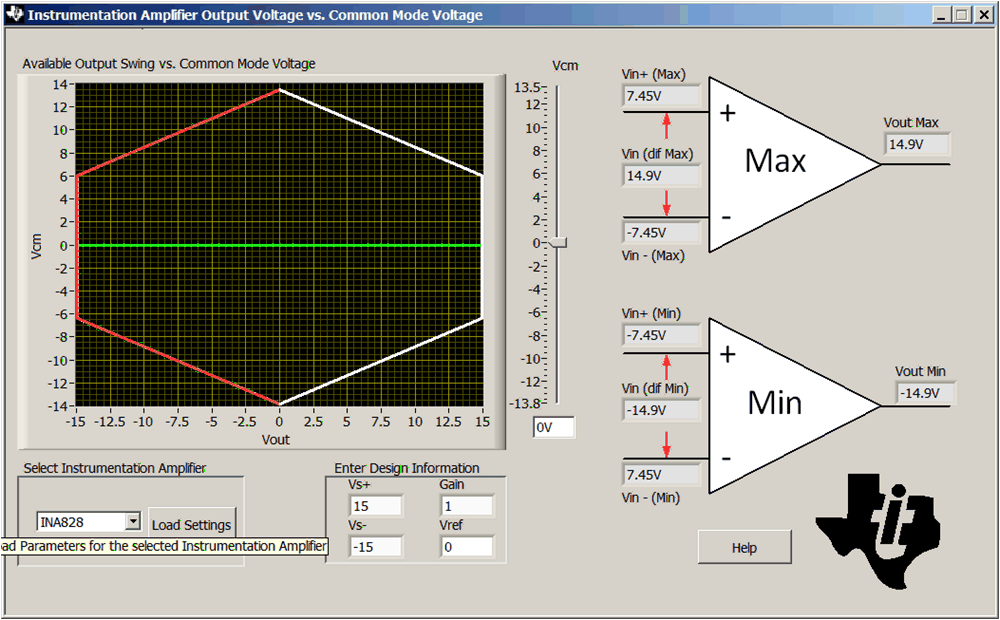
- Check the common mode and output range of the instrumentation amplifier using the Common-Mode Input Range Calculator for Instrumentation Amplifiers software tool.
- Use a COG type capacitor for Cfilt to minimize distortion.
- The Precision Labs video series covers methods for selecting the charge bucket circuit Cflt and Rflt. See the Introduction to SAR ADC Front-End Component Selection for details on this subject.
Component Selection
- The ADS8568 can accept a ±10-V single-ended input signal. The INA828 is used to translate a ±10-V differential signal to a ±10-V single-ended signal. So the INA828 is in unity gain for this example, and no external gain set resistor Rg is needed. See Circuit for Driving an ADC with an Instrumentation Amplifier in High Gain in cases where the input signal range is small and gain is required.
- The INA826 reference voltage (Vref) input is used to shift asymmetrical input ranges to match the input range of the ADC. In this case the input range is symmetrical so the Vref pin is grounded (Vref = 0V). See Circuit for Driving an ADC with an Instrumentation Amplifier in High Gain for an example where the Vref pin is used to adjust asymmetrical input signals.
- Use the Common-Mode
Input Range Calculator for Instrumentation Amplifiers to
determine if the INA828 is violating the common-mode range. The
common-mode calculator in the following figure indicates that the output swing
is ±14.9V for a 0-V common mode input.
- Find the value for Cfilt, and Rfilt using TINA SPICE and the methods described in Introduction to SAR ADC Front-End Component Selection. The value of Rfilt and Cfilt shown in this document will work for these circuits; however, if you use different amplifiers you will have to use TINA SPICE to find new values.
DC Transfer Characteristics
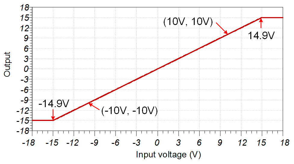
The following graph shows a linear output response for inputs from differential –14.9V to +14.9V. The input range of the ADC is ±10V, so the amplifiers are linear well beyond the required range. See Determining a SAR ADC’s Linear Range when using Instrumentation Amplifiers for detailed theory on this subject. The full-scale range (FSR) of the ADC falls within the linear range of the instrumentation amplifier.
AC Transfer Characteristics
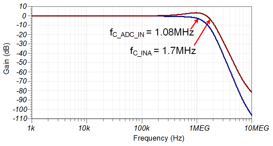
The bandwidth for this circuit is simulated to be 446.75kHz and the gain is 0dB.
Transient ADC Input Settling Simulation (200kSPS)
The following simulation shows settling to a 10-V DC input signal with INA828 and ADS8568. This type of simulation shows that the sample and hold kickback circuit is properly selected to within ½ of a LSB (152µV) at 200kSPS sampling rate on ADS8568. See the ADC Front End Component Selection video series for detailed theory on this subject.
Noise
This section shows a simplified noise calculation for a rough estimate. The bandwidth estimate was taken from the TINA simulation, and the noise density values are from the INA828 50-μV Offset, 7-nV/√ Hz Noise, Low-Power, Precision Instrumentation Amplifier data sheet. The Kn factor of 1.22 is used because the filter is second order (the INA and output filter both have a pole).

Note that simulated and calculated are close but not exact (simulated = 86.6µV, calculated = 103µV). The difference is because the INA has gain peaking and the filter order is approximated as two but in reality the INA and filter poles are not exactly aligned.
Design Featured Devices
| Device | Key Features | Link | Other Possible Devices |
|---|---|---|---|
| ADS8860 | 16-bit resolution, SPI, 1MSPS sample rate, single-ended input, Vref input range 2.5V to 5.0V | 16-bit, 1-MSPS, 1-channel SAR ADC with single-ended input, SPI and daisy chain | Precision ADCs |
| INA826 | Bandwidth 1MHz (G=1), low noise 18nV/√ Hz, low offset ±40µV, low offset drift ±0.4µV/°C, low gain drift 0.1ppm/°C. (Typical values) | Precision, 200-μA Supply Current, 36-V Supply Instrumentation Amplifier | Instrumentation Amplifiers |
Link to Key Files
Texas Instruments, Source Files for SBAA999, support software