SBAA331A January 2019 – August 2024 DAC60501 , OPA207
Design Goals
| DAC Supply Voltage | Amplifier Supply Voltage | DAC Output Range | Output Voltage Range | Output Current Capability | Power-On Reset Output |
|---|---|---|---|---|---|
| 5.5V | ±5.5V | 0V to 2.5V | –5V to 0V | ±20mA | –5V |
Design Description
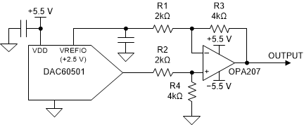
This circuit shows how to convert a positive unipolar digital-to-analog (DAC) output to a negative unipolar output using only an external operational amplifier (op amp) and resistors. In many applications, such as active antenna systems (AAS) and macro remote radio units (RRU), a DAC output is used to bias the gate of gallium nitride (GaN) power amplifier (PA). For these amplifiers to be powered down, a negative potential must be applied to the gate. As such, it is beneficial to have the gate voltage be negative by default. PA biasing applications also require current output source and sink capability that usually exceeds that of most DACs.
These design goals are achieved by utilizing a voltage-output DAC that also features a reference. The DAC output and reference output are connected to differential amplifier with the reference connected to the inverting input. This enables the zero-scale output of the DAC to set the output of the amplifier to its negative full-scale value.

Design Notes
- At power-on, the DAC output will assume a default value. This value can be configured in some devices by connecting a reset-select pin to a high or low potential, which selects a start-up value of zero-scale or mid-scale. In AAS designs, it is beneficial to start at zero-scale to ensure the PA is disabled. Other applications may require a DAC to start at mid-scale.
- The amplifier selected must provide the output current required by the application. Rail-to-rail outputs allow the op amp power supplies to be minimized without clipping the desired output range of the circuit. In AAS applications, there is usually a capacitive load on the output as well, so capacitive load stability is important to consider.
- The op amp must feature a bipolar supply, as the op amp inputs will always be greater than or equal to 0V in operation. The negative supply must be low enough to allow the output to reach its most negative value.
Design Steps
- Select a DAC for the circuit
based on initial on key requirements, such as the resolution, channel count,
output accuracy, and power supply. These performance requirements are variable
and application dependent. However, a few additional items must be considered as
well.
- The reference used to provide the offset of the
differential amplifier will be required to source current. Current will
flow from the reference through the resistors in the feedback network
(R1 and R3) to the output of the amplifier. The maximum current would
occur when the DAC output is at 0V and the output of the amplifier is at
its most negative potential. The following equation shows how to
calculate this current. If the current load is too great for the desired
DAC reference, then a unity-gain buffer can be added to the circuit.

- The output of DAC will also have to drive a resistive
load, comprised of R2 and R4. The maximum required current drive
capability is expressed in the following equation:

- DACs which have an output range from 0V to VREF allow the resolution to be optimized for the negative output.
- The reference used to provide the offset of the
differential amplifier will be required to source current. Current will
flow from the reference through the resistors in the feedback network
(R1 and R3) to the output of the amplifier. The maximum current would
occur when the DAC output is at 0V and the output of the amplifier is at
its most negative potential. The following equation shows how to
calculate this current. If the current load is too great for the desired
DAC reference, then a unity-gain buffer can be added to the circuit.
- The output range of the system can be calculated using the
following equation. This is assuming that R3 and R4 are equal and R1 and R2 are
equal.

- Select resistor values to achieve a balance between output noise and power consumption. Lower resistor values will minimize the thermal noise of the resistors, but increase the power dissipation. The minimum resistance values are limited by the output drive capabilities of the DAC and reference output. The accuracy of the output transfer function is heavily dependent on the accuracy of the resistor ratios. High-accuracy resistors are recommended.
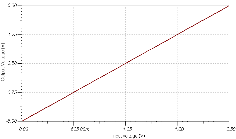
DC Transfer Characteristics
The following simulation shows the output transfer function of the circuit:

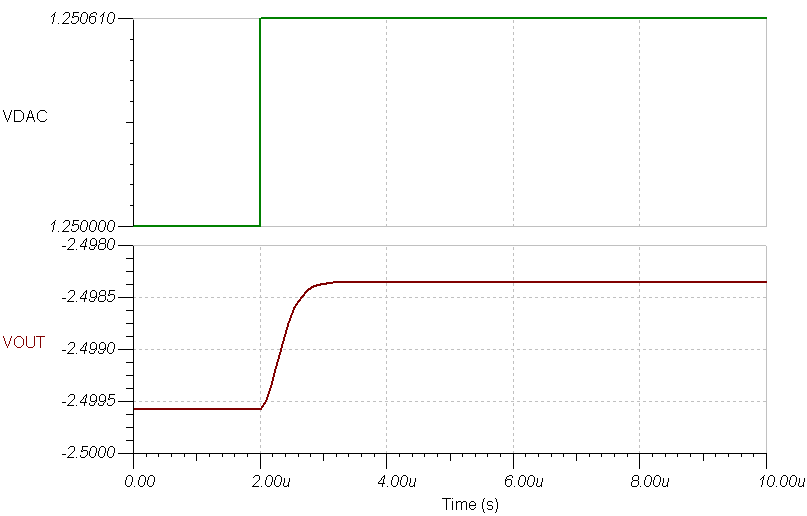
Small-Step Response
The following figure displays an LSB step response of the circuit with 15-pF load on the output.

Design Featured Devices
| Device | Key Features | Link | Other Possible Devices |
|---|---|---|---|
| DAC60501 | 12-bit, 1-LSB, voltage-output digital-to-analog converter with precision internal reference. | True 12-bit, 1-ch, SPI/I2C, voltage-output DAC in WSON package with precision internal reference | Digital-to-analog converters (DACs) |
| OPA207 | Low-power, high-precision, low-noise, rail-to-rail output, operational amplifier | Low power (350µA), low noise (7.5nV/√Hz), high precision (100µV, 0.2µV/⁰C), bipolar RRO op amp | Precision op amps (Vos<1mV) |
Design References
Texas Instruments, companion simulation files for this circuit, software support