SBAA332A January 2019 – September 2024 DAC8871 , OPA211 , OPA828 , REF6050
Design Goals
| DAC Output Range | DAC VREFH Input Voltage | DAC VREFL Input Voltage |
|---|---|---|
| –5V to 5V | 5V | –5V |
Design Description
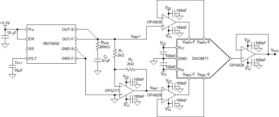
High-precision digital-to-analog converters (DACs) used in applications like magnetic resonance imaging (MRI) machines and arbitrary waveform generators (AWG) generally require a high-precision voltage reference. A cause of common issues with these systems is the undesired series resistance on the reference input of the DAC. The resistance will induce a DAC input-code dependent voltage potential across them as the input current of the R-2R ladder changes based on the code. The end result is that the reference voltage will seem to change based on the DAC code, which will cause a bow shaped integrated non-linearity error curve.
To remedy this issue, high-precision DACs often feature a reference force and sense pin for each of the reference inputs (VREFH and VREFL). While these pins are essentially just two parallel connections with individual series resistance to the reference input nodes of the R-2R ladder, the addition of an external unity-gain reference buffer will allow the voltage at the node to be compensated by the amplifier. The small bias current flowing into the op amp inverting input will generate a minimum voltage across the series resistance of the sense input, while output of the op amp can source the current required by the R-2R ladder.
Design Notes
- The reference selected only has a positive 5-V output, necessitating an inverting amplifier to generate the VREF- value. The resistors R1 and R2 also create a current path from the reference output to a –5V potential. This current is provided by the voltage reference. The current can be limited by increasing the values of R1 and R2, at the expense of additional noise being created by the circuit. The current noise of the amplifier and the thermal noise of the resistors contribute to the total noise of the circuit.
- The noise of the reference is reduced by adding CFILT, which filters the noise generated by the band gap of the internal reference. The output of the reference also requires a capacitor (CL) with a minimum equivalent series resistance (ESR). It is possible to create this resistance on the PCB with an extended trace, shown as RESR.
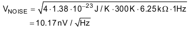
- The noise of the DAC is primarily created by the thermal noise
of the resistor ladder. Thermal noise is calculated using the following the
equation, where Kb is Boltzmann's constant, T is the temperature in
kelvin, R is the resistance of the ladder, and F is the frequency range.
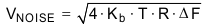
The DAC8871 typical output impedance of approximately 6.25kΩ, and assuming room temperature operation, has a thermal noise that can be calculated as shown in the following equation:
Design Steps
- The DAC is selected for its resolution, accuracy, and noise performance. The resolution may be dependent on the application, but it is common to see 16-bit or greater resolution in this circuit. Errors in the output of the DAC are considered non-linearity errors. Non-linearity errors are expressed as integrated non-linearity error (INL) and differential non-linearity error (DNL). Assuming an ideal reference on the input of the DAC, the INL and DNL errors of the system will be caused by resistor inaccuracies of the R-2R ladder.
- The reference is selected based on the accuracy, thermal drift, and noise requirements of the application. The output voltage accuracy is generally specified as a percentage. The thermal drift is specified in units of ppm/°C (parts-per-million). The noise of the circuit has two specification: the low-frequency noise, usually specified in VPEAK-PEAK over a limited frequency domain (0.1Hz to 10Hz), and the total integrated noise, specified in VRMS.
- The op amp used to invert the reference voltage should be selected on its noise performance. The amplifier will contribute noise to the system in two ways, its voltage noise and current noise. The contribution from the voltage-noise can be minimized by selecting a bipolar input amplifier, which generally have a low voltage noise. Bipolar input amplifiers also have higher current noise than CMOS input amplifiers, but the current noise is converted to voltage noise via the resistors R1 and R2 of the circuit. By minimizing the resistance of those components, the current noise contribution of the amplifier can be minimized.
- The amplifiers selected to drive the force and sense inputs of the DAC should be selected according to fast settling and bandwidth. When the DAC is updated with a new input code, the switches in the R-2R resistor ladder will cause a sudden change in current that is being demanded from the reference inputs. This results in a transient on the reference inputs that will also be conveyed on the DAC output. If the reference buffer amplifiers can settle quickly, the error on the output will be minimized. In addition, the voltage noise of these amplifiers will contribute to the total noise of the system. For this reason a bipolar or JFET input amplifier should be selected.
- Select an output buffer if the circuit is desired to drive a load. The DAC8871 is an unbuffered device, meaning that the output of the DAC is a node on the resistor ladder. This amplifier is selected based on the requirements of the load: such as current output capability, capacitive load stability, slew-rate, and voltage range.
- The capacitors CFILT and CL are low-ESR, ceramic type capacitors. The voltage rating of the capacitors needs to be compliant with the 5-V reference output.
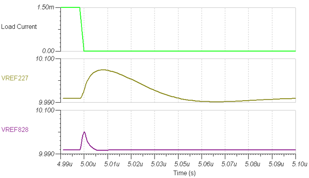
Reference Buffer Load Transient
The reference buffer must be able to quickly source transient currents necessary for the R-2R ladder when the DAC changes codes. Given the architecture of the DAC8871, the maximum transient current would occur when the DAC transitions from zero- or full-scale code to the mid-scale. This transient is simulated with a current source between the VREFH and VREFL inputs. The following simulation shows the differential reference voltage during the current transient, simulated with the OPA828 and OPA227. This shows that the reference error magnitude and duration is reduced with the OPA828.
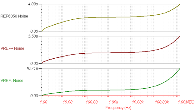
Reference Buffer Total Noise
The total noise generated by the circuit is shown in the following simulation. The reference, inverting amplifier, and reference buffers each contribute to the noise. Note that the VREF- input has greater noise due to the contribution of the inverting amplifier and the discrete resistors in its feedback network.
Design Featured Devices
| Device | Key Features | Link | Other Possible Devices |
|---|---|---|---|
| DAC8871 | 16-bit, single-channel, serial-interface, high-voltage, bipolar-output DAC | 16-Bit Single Channel, Serial Interface, ±18V (High Voltage Bipolar) Output DAC | Precision DACs (≤10 MSPS) |
| OPA828 | Low-offset, low-drift, low-noise, 45-MHz bandwidth, JFET-input operational amplifier | High-speed (45MHz and 150V/μs), 36V, low-noise (4nV/√Hz) RRO JFET operational amplifier | Precision op amps (Vos < 1mV) |
| OPA221 | Low-power, 1.1nV/√Hz noise, high-performance operation amplifier | 1.1nV/rtHz Noise, Low-Power, Precision Operational Amplifier | Precision op amps (Vos < 1mV) |
| REF6050 | Low-noise, high-precision, 5-V output voltage reference | 5V, 5ppm/°C high-precision voltage reference with integrated buffer and enable pin | Series voltage references |