SBAA333A January 2019 – September 2024 OPA1612 , PCM1794A , PCM1794A-Q1
Design Goals
| DAC IOUT Amplitude | DAC IOUT Common Mode Current | VOUT Amplitude |
|---|---|---|
| 7.8mAP-P | –6.2mA | 2.1VRMS |
Design Description
Many high-performance audio digital-to-analog converters (DACs) feature a current output that must be converted into a voltage output for use with audio amplifiers. In premium automotive audio applications, for example, it is critical that the DAC signal-to-noise ratio (SNR) and total harmonic distortion plus noise (THD+N) performance is not compromised by the current-to-voltage (I-V) output stage.
Design Notes
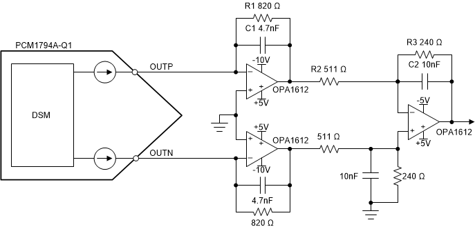
- The first stage of the circuit converts the current output to a voltage output by providing a virtual ground potential to the OUTP and OUTN nodes of the DAC. The current flowing from the DAC then creates a voltage across the resistor, R1, in the feedback loop. Note that current-output audio DACs have a common-mode current that creates an offset to confirm that the DAC is always sourcing current. This common-mode current also results in the output of the first stage always being a negative value. The supplies of the amplifiers of the circuit are not required to be symmetrical.
- The second stage of the circuit is a differential amplifier that converts the differential voltage of the first stage into a single-ended output voltage.
Design Steps
- The DAC is selected based on the needs of the application. Consider the required SNR, THD+N, and supported I2S interface sample rates. While most audio DACs support rates ranging from 16kHz to 192kHz, not all support rates like 384kHz or 768kHz. Higher rates result in noise shaping that moves the out-of-band noise further from the audible range, but not all audio sources can provide them. Also note that not all current-output audio DACs have the same amplitude and common-mode current.
- Select the amplifier based on its noise and THD performance. These amplifiers must not gate the SNR performance of the DAC. A JFET or bipolar-input amplifier is recommended for its low voltage-noise. The higher current-noise is not an issue as the resistance values of the circuit are low.
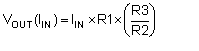
- The gain of the circuit is calculated with the following equation. Using R1 = 820Ω, R2 = 511Ω, and R3 = 240Ω, the output voltage will be approximately 6VP-P or 2.1VRMS. For this circuit, preferable noise performance is achieved by having the first stage have a large gain, and the second stage actually attenuate the signal.
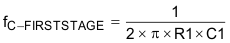
- The cutoff frequency (fC) of the first stage can be calculated with the following equation:
The fC of the second stage is calculated with the following equation:
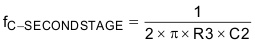
Using C1 = 4.7nF and C2 = 10nF, the fC of the first stage is approximately 44.2kHz and the fC of the second stage is approximately 66.3kHz.
- The capacitors used for the filter should be COG/NP0 type ceramics. COG/NP0 type capacitors have a lower voltage coefficient of capacitance, meaning that the capacitive value of the component is less impacted by the voltage bias across the device. As the capacitors are key for performance of the filter, other types of ceramic capacitors should be avoided in the signal path.
- Thin-film resistors are recommended for the resistive elements in the circuits. All resistors feature voltage noise, which is well understood to be dependent on resistance and temperature, as shown in the first equation that follows. But resistors also have a current-noise, which is dependent on the voltage across the resistor, frequency, and a constant, C, that is dependent on the material of which the resistor is composed, as shown in the second following equation: ST = 4kRT,
where
- k is Boltzmann's constant
- R is resistance
- T is temperature
SE = ( C × U2 ) ÷ ƒwhere
- C is a constant derived from the resistor material
- U is the differential voltage across the resistor
- ƒ is the frequency
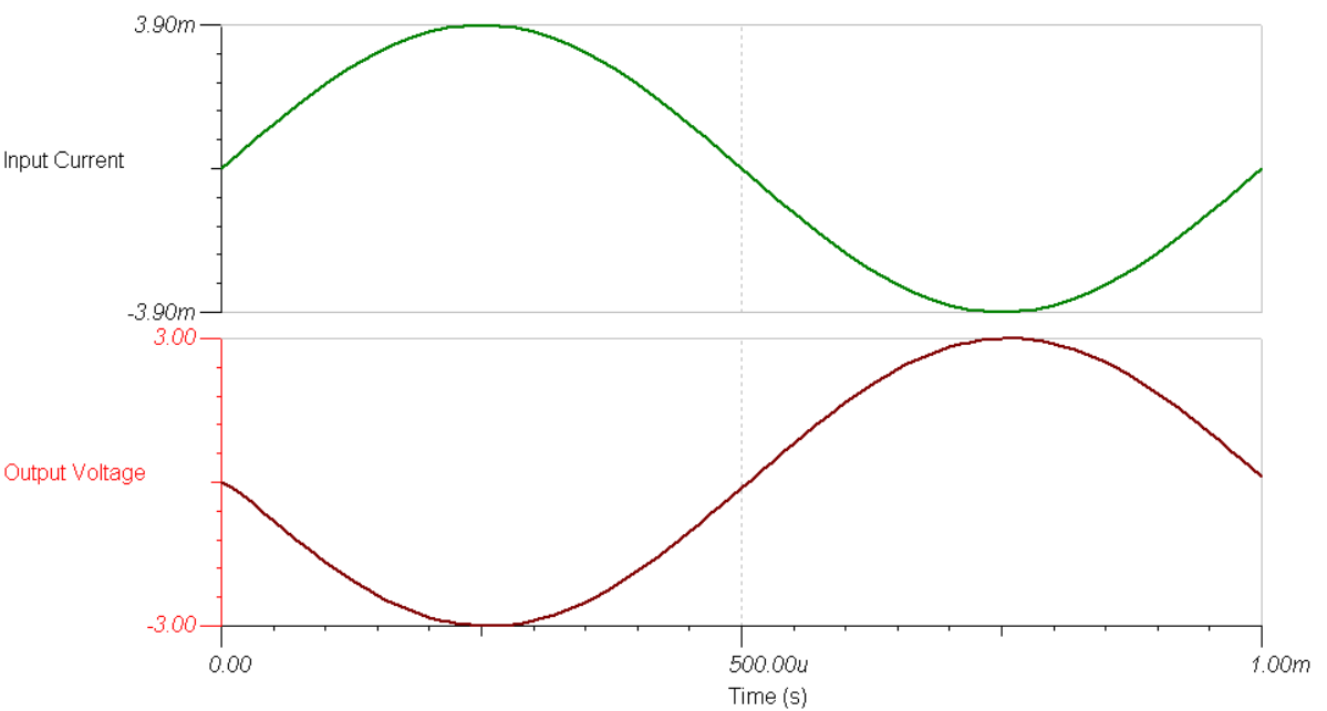
DC Transfer Characteristics
The simulation shows that the 7.8mAP-P differential input current results in an approximately 6VP-P output, or 2.1VRMS.
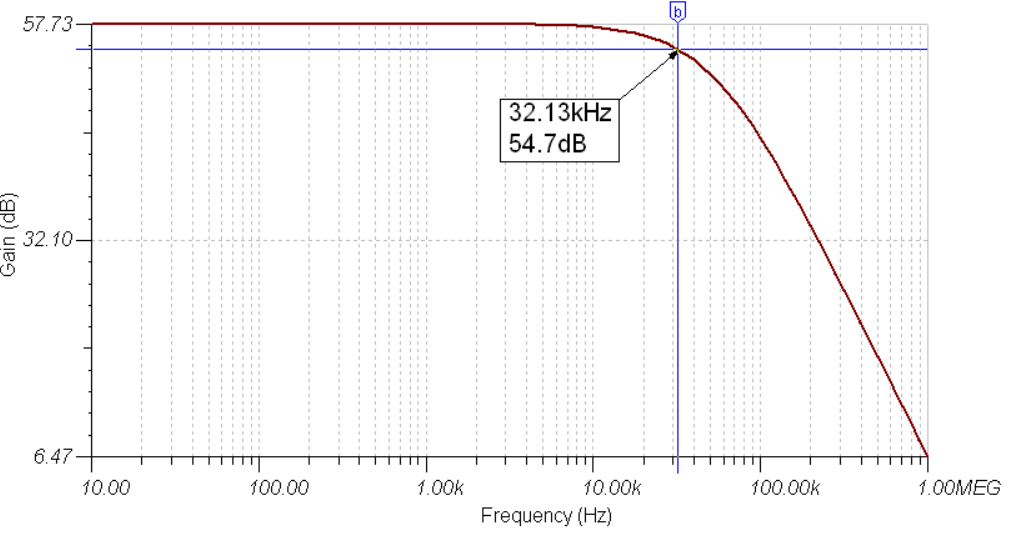
Filter Characteristics
The filters created by the two amplifier stages have a –3dB corner frequency of approximately 32.1kHz. This attenuates out-of-band noise from the output, while not affecting the audible range (20Hz to 22kHz).
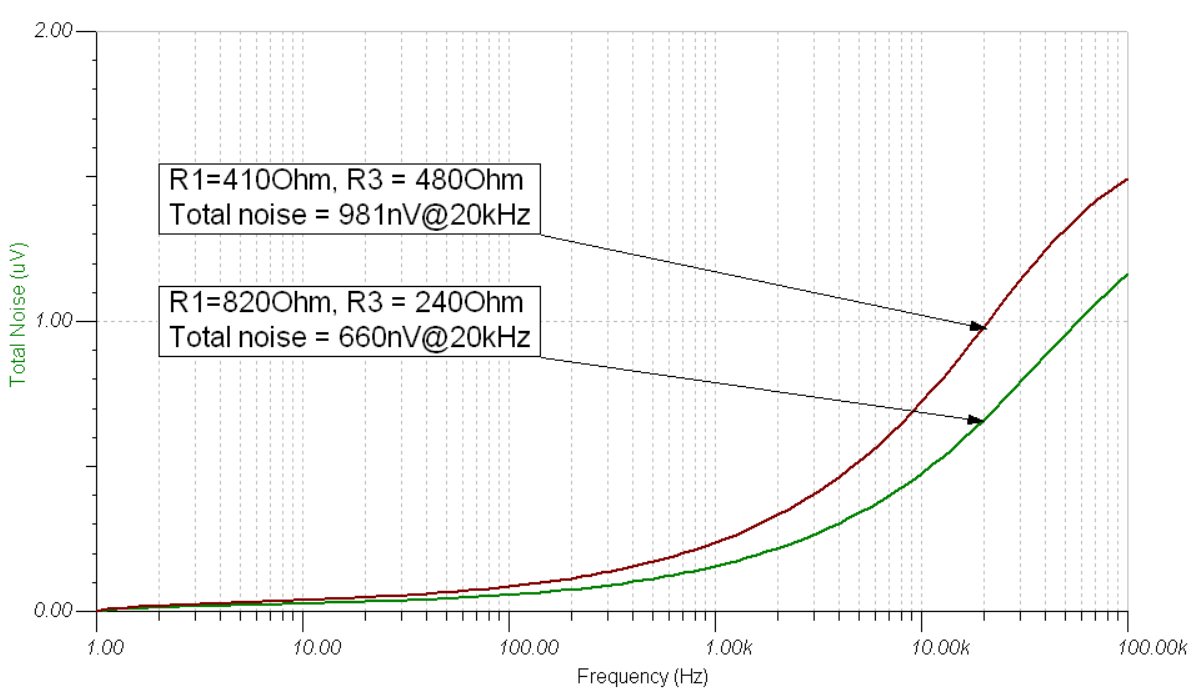
Noise Simulation
The following simulation shows the benefit of having the majority of the gain of the circuit in the first stage. The two curves were generated by the same circuit with different resistor values, but resulting in the same total gain. The green line has a higher gain in the first stage, but lower total noise.
Design Featured Devices
| Device | Key Features | Link | Other Possible Devices |
|---|---|---|---|
| PCM1794A-Q1 | 24-bit, 192-kHz sampling, advanced segment, audio stereo digital-to-analog converter | 132dB, 24-bit, 192-kHz advanced Segment, Audio Stereo Digital-to-Analog Converter | Audio DACs |
| OPA1612 | Ultra-low noise, ultra-low distortion, high-performance, bipolar-input audio operational amplifier | SoundPlus™ Audio Operational Amplifier with 1.1nV/√Hz Noise, Low THD and Precision | Audio Op-Amps |
Design References
Texas Instruments, HiFi Audio circuit design, application report
Texas Instruments, SBAM413 circuit, simulation files
Other Links:
Texas Instruments, Precision DAC Learning Center, portfolio overview
Texas Instruments, Audio DACs, portfolio overview