SBAA340A January 2018 – September 2024 ADS7040 , ADS7041 , ADS7042 , ADS7056 , INA190 , INA190-Q1
| Input | ADC Input | Digital Output ADS7042 |
|---|---|---|
| –6A | 0.3V | 19AH, 410d |
| +6A | 2.7V | E66H, 3686d |
| AVDD / VREF | DVDD | Vsup |
|---|---|---|
| 3.0V | 1.65V | 40V |
Design Description
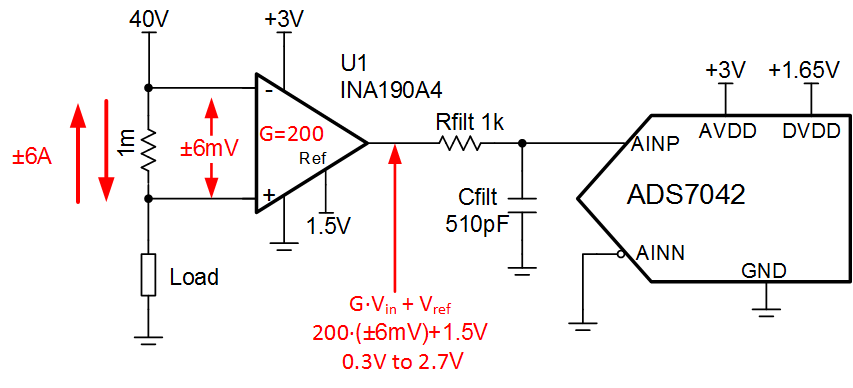
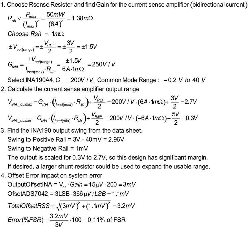
Current shunt monitors are amplifiers that are optimized to read small shunt voltages over very wide common mode ranges. This example application uses the INA190A4 to translate a ±6-A current into a 0-V to 3-V range for the ADC. Note that this is a high sided current measurement with a 40V common mode range. Detailed theory on current sensing is covered in Using current sense amplifiers to solve today’s current sensing design challenges. Compared to other current shunt devices the INA190 has very low offset voltage, bias current, and drift. This excellent DC performance allows smaller for smaller input voltage ranges without compromising accuracy as the offset is small compared to the input signal. The use of small shunt resistors is an advantage as the power dissipated in the shunt is smaller for smaller resistors for a given current level. The ADS7042 is a 12-bit 1MSPS SAR ADC with a 3V analog input range. The design shown in this document can be modified for other data converters and input ranges. This design can be used a wide range of applications where current needs to be monitored such as notebook computers, cell phones, and battery management.
Specifications
| Specification | Goal | Calculated | Simulated |
|---|---|---|---|
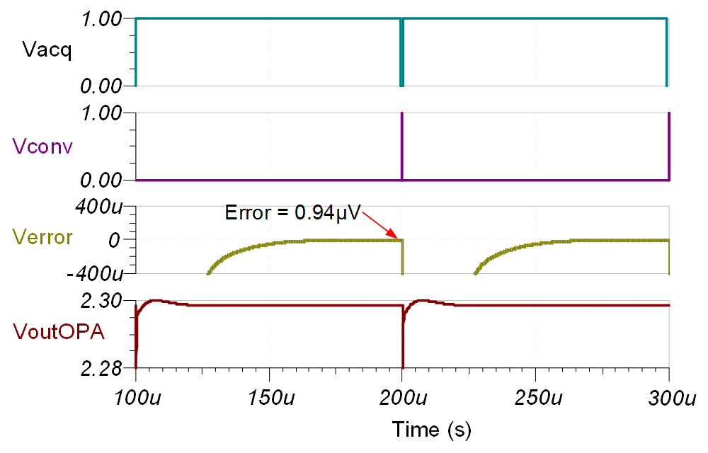
| Transient Settling | < 0.5LSB = 366µV | NA | 0.94µV |
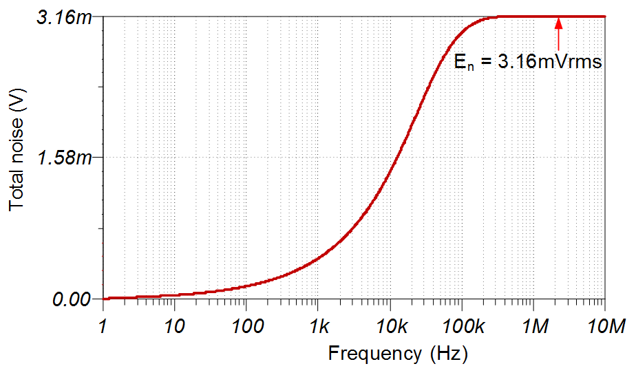
| Noise | NA | 3.5mVrms | 3.16mV |
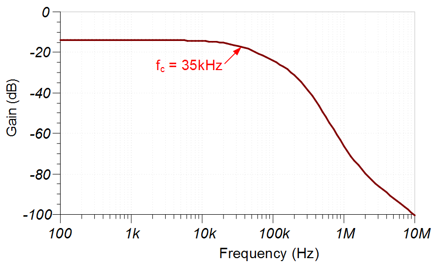
| Bandwidth | NA | 33kHz | 35kHz |
Design Notes
- The tolerance in the shunt resistor, RSENSE, will translate into a gain error. Choose the tolerance according to your error budget. Note that the maximum specified gain error for the INA190A4 is 0.3% and a common tolerance 1-m resistor is 0.5% to 1.0%.
- Selection of the shunt resistor is covered in the component selection section. The objective is to minimize power dissipation while maintaining good accuracy.
- Use a C0G capacitor for CFILT to minimize distortion.
- The example design is for a bidirectional current source (for example, ±6A). A similar approach can be followed for an unidirectional current source (for example, 0A to 12A). The main difference is that the reference input pin would connect to ground as opposed to 1/2 VREF.
Component Selection
DC Transfer Characteristics
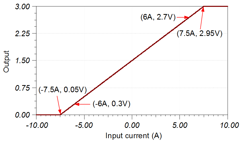
The following graph shows a linear output response for inputs from –7.5A to +7.5A. The required linear range is ±6A, so this circuit meets the requirement with design margin.
AC Transfer Characteristics
The data sheet specified bandwidth of 33kHz for the INA190A4 closely matches the simulated 35kHz bandwidth. The input ADC filter is designed to minimize charge kickback and does not limit the bandwidth ( fc(ADC filter) = 312kHz ). See TI Precision Labs - Op Amps: Bandwidth 1 for more details on this subject.
Transient ADC Input Settling Simulation
The transient ADC simulation is performed for a near full scale input (VinADC = 2.3V), for a 100-kHz sampling rate. Note that the sampling rate needed to be adjusted as the INA190 does not have sufficient bandwidth to respond to the transient charge kickback from the ADC at full sampling rate. Refer to Introduction to SAR ADC Front-End Component Selection for detailed theory on this subject.
Noise Simulation
The noise hand calculation follows. This calculation assumes that the filter is a first order but inspection of the bandwidth simulation shows a more complex response.
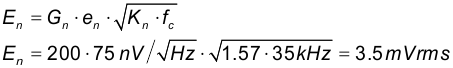
Note that the calculated and simulated match well. Refer to TI Precision Labs - Op Amps: Noise 4 for detailed theory on amplifier noise calculations, and Calculating the Total Noise for ADC Systems for data converter noise.
Design Featured Devices
| Device | Key Features | Link | Other Possible Devices |
|---|---|---|---|
| ADS7042 | 12-bit resolution, SPI, 1MSPS sample rate, single-ended input, AVDD/Vref input range 1.6V to 3.6V. | 12-Bit 1MSPS Ultra-Low-Power Ultra-Small-Size SAR ADC With SPI Interface | Analog-to-digital converters (ADCs) |
| INA190 | Low Supply voltage (1.7V to 5.5V), Wide Common-Mode (-0.2V to 40V), Low Offset Voltage (Vos < 15µV Max), Low Bias Current (500pA typ). | 40-V, Bidirectional, Ultraprecise Current Sense Amplifier with Picoamp IB and ENABLE | Analog current-sense amplifiers |
Link to Key Files
Texas Instruments, TINA source files, software support