SBAA371A June 2019 – September 2024 ADS7056 , LMH6642 , LMH6643 , LMH6643Q-Q1 , LMH6644 , OPA192 , OPA2863 , OPA2863A , OPA365 , OPA863 , OPA863A
| Input | ADC Input | Digital Output ADS7056 |
|---|---|---|
| VinMin = 0V | AIN_P = 0V, AIN_M = 0V | 000H or 010 |
| VinMax = 10V | AIN_P = 3.3V, AIN_M = 0V | FFFH or 409610 |
| Vcc | AVDD | DVDD |
|---|---|---|
| 12V | 3V | 1.65V |
Design Description
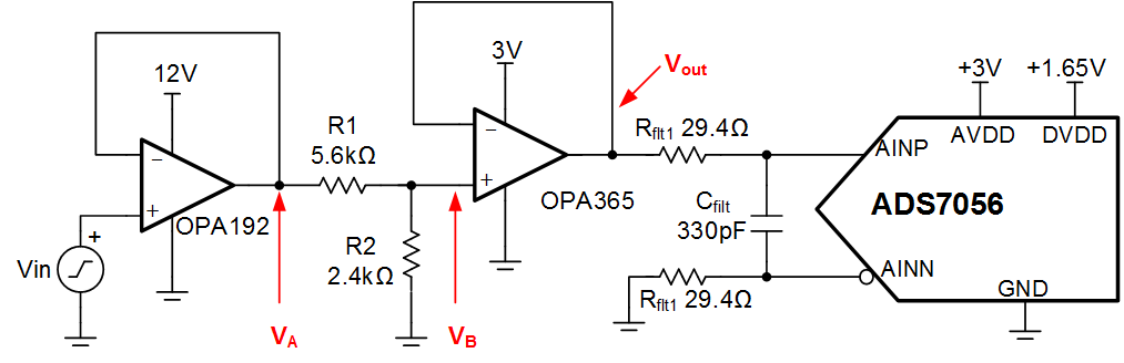
This design is meant for increases the input range of a low-power SAR ADC by attenuating the input signal to match the full-scale range. The values in the component selection section can be adjusted to allow for a different input voltage range on the amplifier and full-scale range on the ADC. The input signal in this design is first buffered by the OPA192 device, a high-voltage precision amplifier, to avoid gain errors from the signal source impedance. A resistor divider at the output of the OPA192 device is then used to attenuate the signal and is again buffered by the OPA365 device. This wide-bandwidth amplifier allows the ADS7056 device to be used at a max sampling rate of 2.5MSPS. This circuit implementation is applicable to test and measurement, appliances, and factory automation and control. In general, this circuit can be used for most applications where a higher voltage signal needs to interface with a low-voltage single-ended ADC.
Specifications
| Specification | Goal | Calculated | Simulated |
|---|---|---|---|
| Transient ADC Input Settling | < 0.5 × LSB = 91.5µV | 16µV | |
| Bandwidth | > 5MHz | 8.09MHz | 7.04MHz |
| Noise | < 0.5 × LSB | 20.85µVRMS | 22.74µVRMS |
Design Notes
- The input amplifier (OPA192) needs a common mode range from 0V to 10V. Since the negative supply is grounded, input swing to the negative rail or a rail-to-rail amplifier is required. The OPA365 device has a similar rail-to-rail requirement.
- The output swing of the amplifiers limits the usable range near ground. Use a small negative supply (for example, –0.3V) to provide output swing to ground. See Powering a dual-supply op-amp circuit with one LDO for a circuit to generate this supply.
- Select C0G capacitors for Cfilt to minimize distortion.
Component Selection
- Find the maximum and minimum output
for the linear operation of the input buffer OPA192. Use this with the gain in
step 3 to calculate the overall linear range of the OPA192 device.
- (V–) – 0.1V < VA < (V+) + 0.1V from OPA192 Vcm specification
- (V–) + 0.110V < VA < (V+) – 0.110V from OPA192 Vout swing specification
- (V–) + 0.3V < VA < (V+) – 0.3V from OPA192 Aol linear region specification
- Combining the limitations, the overall range is (V–) + 0.3 V < VA < (V+) – 0.3V
- Replacing (V–) = 0V and (V+) = 12V for the OPA192 supplies, the limit is 0.3V < VA < 11.7V
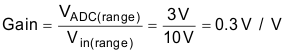
- Find the gain based on input signal
and ADC full-scale input range
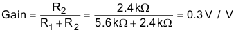
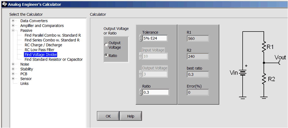
- Find standard resistor values for
voltage divider to provide gain. Use the Analog engineer’s calculator to find standard values for
voltage divider ratio.
- The linear range for VB consists of the range found in step one multiplied by our gain. The range is therefore: 0.09V < VB < 3.51 V.
- Maximum and minimum output for
linear operation of the OPA365:
- (V–) – 0.1V < Vout < (V+) + 0.1V from OPA365 Vcm specification
- (V–) + 0.02V < Vout < (V+) – 0.02V from OPA365 Vout swing specification
- (V–) + 0.1V < Vout < (V+) – 0.1V from OPA365 Aol linear region specification
- Combining the limitations, the overall range for OPA365 is (V–) + 0.1V < Vout < (V+) – 0.1V
- Replacing (V–) = 0V and (V+) = 3V for the OPA365 supplies, the limit is 0.1V < VA < 2.9V
- Combining the range from the OPA192 and the OPA365:
- Find Rfilt and Cfilt to allow for settling at 2.5MSPS. See the TI Precision Labs – ADCs: Refine the Rfilt and Cfilt Values video showing the algorithm for selecting Rfilt and Cfilt. The final value of 29.4Ω and 330pF proved to settle to well below ½ of a least significant bit (LSB).
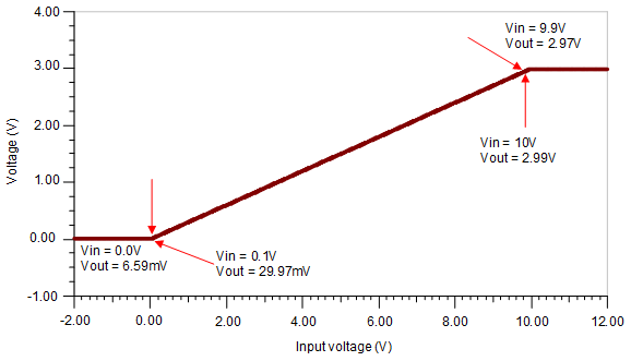
DC Transfer Characteristics
The following graph shows a linear output response for inputs from 0V to 10V. The image shows there is degraded performance towards both AVDD and ground. This is due to the linear ranges of the amplifiers in the Component Selection section. To improve performance at these extremes, the power supplies can be adjusted so that the linear range of both amplifiers fall within the full-scale range of the ADC.
AC Transfer Characteristics
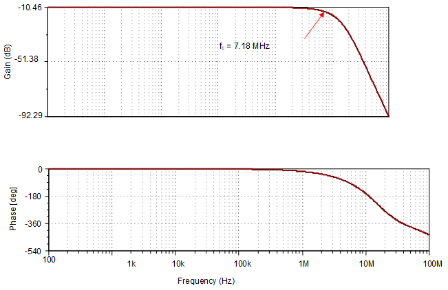
The bandwidth is simulated at approximately 7MHz at the –3dB point. The bandwidth is limited by both the OPA192 device and the RC charge bucket circuit (Rfilt and Cfilt). The bandwidth of the RC circuit is shown in the following equation to be 8.2MHz. The OPA192 device has a 10-MHz bandwidth which also affects the overall bandwidth of the circuit. The bandwidth goal was selected to be two times greater than that of the sampling frequency to allow for proper settling.

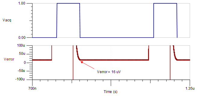
Transient ADC Input Settling Simulation
The following simulation shows settling for a 9-V DC input signal. This type of simulation shows that the sample and hold kickback circuit is properly selected to within ½ of a LSB (91.5µV). See the Introduction to SAR ADC Front-End Component Selection video for detailed theory on this subject.
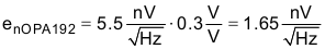
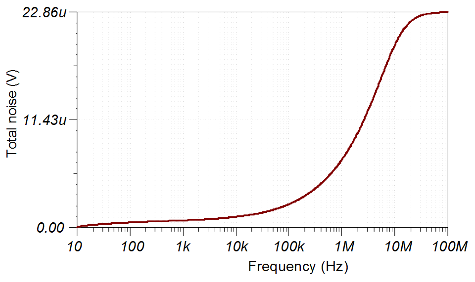
Noise Simulation
This section details a simplified noise calculation for a rough estimate. Noise from the OPA192 is attenuated by the resistor divider as shown:
Resistor divider noise:

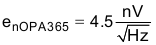
OPA365 noise density:
Total noise:
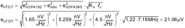
Note that calculated and simulated values match well. See the Calculating the Total Noise for ADC Systems video for detailed theory on this subject.
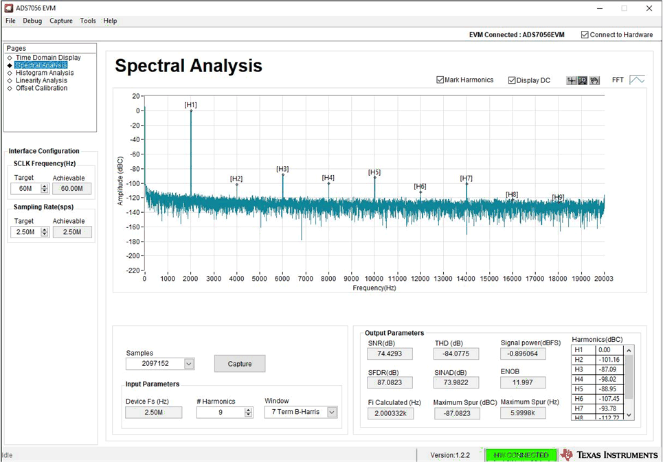
Measured AC Results (FFT)
This performance was measured on a modified version of the ADS7056EVM with a 2-kHz input sine wave. The AC performance indicates SNR = 74.4dB, and THD = –84.07dB, which matches well with the specified performance of the ADC, SNR = 74.9dB and THD = –85dB. This test was performed at room temperature. See the Introduction to Frequency Domain video for more details on this subject.
| Parameter | Data Sheet Specification (Typ) | Measured Result |
|---|---|---|
| SNR | 74.9dB | 74.4dB |
| THD | –85dB | –84.07dB |
Design Featured Devices and Alternative Parts
| Device | Key Features | Link | Other Possible Devices |
|---|---|---|---|
| ADS7056 | 14-bit resolution, SPI, 2.5-MSPS sample rate, single-ended input, AVDD/VREF input range 2.35V to 3.6V, DVDD 1.65V to 3.6V | 14-bit 2.5-MSPS ultra-low-power ultra-small-size SAR ADC with SPI | Precision ADCs |
| OPA192 | 8-kHz bandwidth, rail-to-rail output, 450-nA supply current, unity gain stable | High-Voltage, Rail-to-Rail Input/Output, 5µV, 0.2µV/˚C, Precision Operational Amplifier | Operational amplifiers (op amps) |
| OPA365 | 50-MHz bandwidth, rail-to-rail output, zero-crossover, low offset 100µV, low noise 4.5nV/√ Hz, slew rate 25V/µs | 2.2V, 50MHz, Low-Noise, Single-Supply Rail-to-Rail Operational Amplifier |
Link to Key Files
Texas Instruments, SBAA371 sources files, tool support