SBAA373A June 2019 – August 2024 ADS8860 , LM7705 , OPA320
| Input Power Supply | Output Power Supply |
|---|---|
| 3V to 5.25V | -0.232V |
Design Description
This circuit document shows how to create a small negative power supply (–0.232V) using the LM7705 low-noise negative bias generator with a single 3V to 5.25V power supply. The –0.232V supply is typically used for the negative supply on a single-supply amplifier to allow swing all the way to 0V. Note that amplifiers cannot swing all the way to the power supply rails, but become distorted and clip as they approach the negative rail. For example, based on the OPA320 device, worst-case specifications, it can clip 20mV from the negative supply and can become nonlinear 100mV from the negative supply. If the negative supply is ground, the amplifier output may be distorted below 100mV and will likely clip below 20mV. Otherwise, if the negative supply for the OPA320 op amp is set to a small negative voltage (–0.232V), the output will linear all the way to ground. This circuit can be used for any application where a single-supply amplifier needs to swing to 0V. The LM7705 converts a positive 3V to 5V rail to a negative voltage using a switched capacitor voltage inverter. A related circuit document, Powering a dual-supply op-amp circuit with one LDO, shows a similar circuit.
Specifications
| Specification | Measured: Negative Supply = GND, Positive Supply = 5.2V, VIN = 5Vpp (full-scale signal) | Measured: Negative Supply = –0.232V, Positive Supply = 5.2V, VIN = 5Vpp (full-scale signal) |
|---|---|---|
| THD (of ADS8860 + OPA320) | –93.2dB | –112.5dB (using LM7705) |
Design Notes
- All of the measured results in this document were done using the component values shown on the first page. The previous table shows the performance of an ADS8860 + OPA320 device with and without the LM7705 device. For this example configuration, the input signal is intentionally driven very close to the full-scale input range for the ADC.
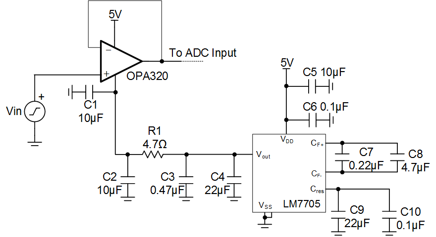
- This circuit uses a switched capacitor inverter to generate a negative supply voltage with a positive input supply voltage. Doing this inversion generates power-supply ripple and noise. This noise is typically small and has minimal impact on system performance. Nevertheless, if this system has a negative power supply, consider using the TPS7A39 LDO to generate a (–0.2V power supply). See Powering a dual-supply op-amp circuit with one LDO for details. Comparing the LDO solution (TPS7A39) to the switched capacitor inverter (LM7705), the LDO will generally be the lowest noise. Use the switched capacitor inverter in cases where the system does not have a negative supply.
Component Selection
- See the LM7705 Low-Noise
Negative Bias Generator Data Sheet for details on component
selection. A key concern for this circuit is the clock feed-through noise from
the LM7705 device. Minimize this noise by choosing larger capacitors (see the
following graph). The trade-off for selecting the large capacitors is the size,
cost, and complexity of the design.
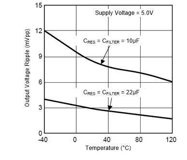
Output vs Input for Typical Amplifier
The following graph shows the output swing limitation for a typical single-supply CMOS op amp as the output approaches 0V. Notice that the amplifier becomes nonlinear about 0.1V from the negative power supply rail. Also, notice that the output saturates (or clips) at 0.25V from the negative rail. Using a small negative supply (–0.232V) eliminates this problem, and the output follows the ideal curve.
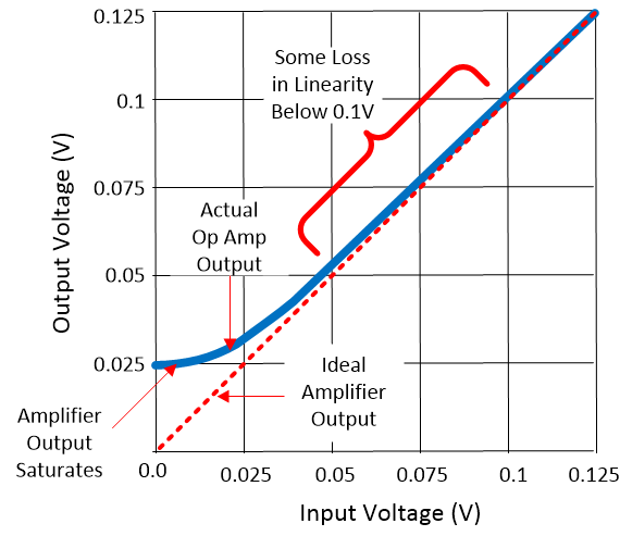
Clipping From Swing Limitations on Negative Rail
This graph shows how the output swing limitation will distort or clip a sinusoidal waveform as it approaches ground. For this example a 5Vpp signal is applied to the input of an op amp with the negative supply connected to GND and –0.232V. The positive supply is connected to 5.2V so there is not an output swing limitation for the positive supply. Notice that the output signal for the amplifier with the grounded negative supply is distorted near ground, whereas the amplifier with the –0.232V negative supply is not distorted near ground.
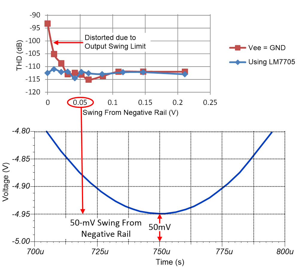
Measured Distortion vs Swing to Rail With and Without the LM7705
This graph shows the measured THD for an OPA320 op amp driving an ADS8860 SAR ADC with a –0.232V negative supply (LM7705) and a grounded negative supply. This curve shows that the amplifier output is distorted when the swing from the power supply rail is less than 50mV for the 0-V negative supply, whereas it is not distorted for the –0.232-V supply.
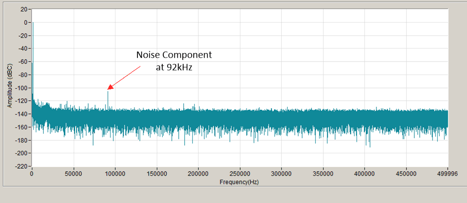
Measured FFT Showing LM7705 Switching Noise
The following FFT chart shows the measured performance for an OPA320 op amp driving an ADS8860 SAR ADC using an LM7705 device to generate the –0.232V supply. The key point here is that the noise from the switched capacitor inverter signal is visible at 92kHz. This noise is relatively low and has little impact on SNR and THD for the device.
| Device | Key Features | Link | Other Possible Devices |
|---|---|---|---|
| LM7705 | Switched capacitor voltage inverter, regulated output voltage −0.232 V, output voltage ripple 4 mVPP, supply voltage 3 V to 5.25 V | Low Noise Negative Bias | TPS7A3901 |
| ADS8860 | 16-bit resolution, SPI, 1-MSPS sample rate, single-ended input, VREF input range 2.5V to 5.0V. | ADS7042 | ADCS |
| OPA320 | 20-MHz bandwidth, rail-to-rail with zero crossover distortion, VOS (MAX) = 150μV, VOS (DriftMAX) = 5μV/°C, en = 7nV/√ Hz | OPA320 | OPAMPS |
Design References
See Analog Engineer's Circuit Cookbooks for TI's comprehensive circuit library.