SBAA375A June 2019 – September 2024 ADS8860 , LMH6642 , LMH6643 , LMH6643Q-Q1 , LMH6644 , OPA2863 , OPA2863A , OPA365 , OPA863 , OPA863A
| Input | ADC Input | Digital Output ADS8860 |
|---|---|---|
| –10V | 0.1V | 0889H or 2185d |
| +10V | 2.9V | F777H or 63351d |
| Power Supplies | |||
|---|---|---|---|
| Vref1 | Vref2 | AVDD | DVDD |
| 1V | 3V | 3V | 3V |
Design Description
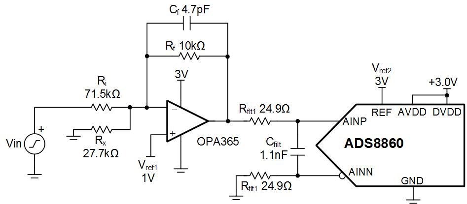
This circuit document describes how to translate a high-voltage signal (for example, ±10V) to low-voltage ADC inputs (for example, 0V to 3V). This circuit does not require any high-voltage supply to operate, but rather uses a voltage divider and level shift to translate the input signal. This circuit shows the OPA365 and ADS8860 devices, but the topology could be applied to many different ADCs. This design can be used a wide range of applications where a high-voltage input needs to be translated such as analog input modules for PLCs, instrumentation (lab, analytical, field and portable), and factory automation and control.
Specifications
| Specification | Goal | Calculated | Simulated |
|---|---|---|---|
| Sampling rate | 1MSPS (max sampling rate) | 800kSPS | |
| Bandwidth | > 1MHz | Poles at 3.39MHz and 4.92MHz | 2.44MHz |
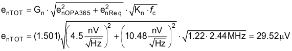
| Noise | < 1/2LSB = 38.1µV | 29.52µV | 31.55µV |
| Transient settling error | < 1/2LSB = 38.1µV | –2.2µV |
Design Notes
- The common mode of this circuit is kept at a constant value (Vref1 = 1V in this example). Because the common mode is constant, the amplifier does not need to have a rail-to-rail input or zero crossover distortion. See the TI Precision Labs Determining a SAR ADC’s Linear Range when using Operational Amplifiers video for more details.
- Select a C0G type capacitor for Cfilt to minimize distortion.
- Use 0.1% 20ppm/°C film resistors, or better, to minimize gain error and drift.
- The input impedance of this circuit is Rin = Ri (71.5kΩ, in this example). For a high-impedance input, use a high-voltage amplifier buffer (for example, Vcc = +15V, and Vee = –15V). Alternatively, the input impedance could be increased by multiplying Ri, Rx, and Rf by the same factor. However, increasing the resistance on all the resistors will impact system noise.
- The TI Precision Labs - ADCs video series covers methods for selecting the charge bucket circuit, Cflt and Rflt. See the Introduction to SAR ADC Front-End Component Selection video for details on this subject. In this example, the sampling rate was reduced from 1MSPS to 800kSPS, to improve settling.
Component Selection
- First select the amplifier input and output range. In this example, the input range is –10V to +10V. The amplifier output range is set according to the ADC input and the amplifier linear output range. The ADC input range in this example is set by the reference voltage and is 3V. The amplifier supply is set to 3V to match the ADC input range. The output of the amplifier cannot swing to the power supply rails because of output swing limitations (that is, the linear range for the OPA365 device is 0.1V < VOUT < 2.9V). The output range can be adjusted further to provide design margin. For example, 0.2V < VOUT < 2.8V, provides margin for issues like power-supply variation.
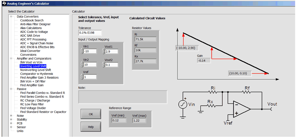
- The Analog Engineer's Calculator can be used in the next step
to select component values. Enter the input and output voltages and reference
voltage (–10V < Vin < +10V, and 0.1V < Vout < 2.9V). The range of
acceptable reference voltages is given at the bottom of the tool (0.12V to 1.22V
in this example). In this example, the reference is selected to be 1V. The tool
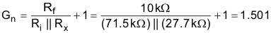
outputs the 0.1% resistors required to map the voltages (Ri = 71.5kΩ,
Rx = 27.7kΩ, Rf = 10kΩ).
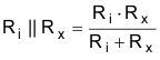
- The
following equations show the transfer function for the inverting level-shift
topology. It is possible to use these equations to solve for the different
component values rather than the calculator. To do this, choose a reference
value and fix the value of Rf to 10kΩ. Once done, solve for Ri and
Rx for two different values of output signal. The algebra for
this problem is a little complex, so using the calculator is the suggested
method. Use the following equations to verify the transfer function:
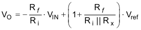
where
-
Using the values from the calculator:
Ri = 71.5kΩ, Rx = 27.7kΩ, Rf = 10kΩ, Vref1 = 1.0VVO = –0.1399V × VIN + 1.5009VVO(–10V) = 2.8995VVO(+10V) = 0.0123V
-
- Find Rfilt and Cfilt to allow for settling at 1MSPS. The Refine the Rfilt and Cfilt Values video shows the algorithm for selecting Rfilt and Cfilt. The final value of 24.9Ω and 1.1nF proved to settle to well below ½ of a least significant bit (LSB).
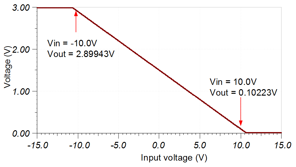
DC Transfer Characteristics
The following graph shows the linear output response for a –10-V to 10-V input. In this case, the amplifier output is approximately 2.9V for a –10-V input and 0.1V for a +10-V input. This design was scaled so that the output range avoids the nonlinear power supply rails by 0.1V. See the Determining a SAR ADC's Linear Range when using Operational Amplifiers video for detailed theory on this subject.
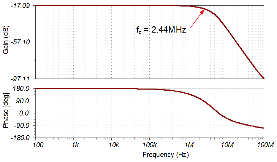
AC Transfer Characteristics
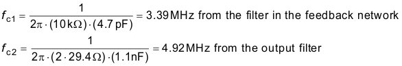
The bandwidth is limited by the Cf × Rf filter (fc1 = 3.39MHz) and the output filter (fc1 = 4.92MHz). These two poles combine to form a second-order filter with a simulated cutoff frequency at 2.44MHz. See the Op Amps Bandwidth video series for more details on this subject.
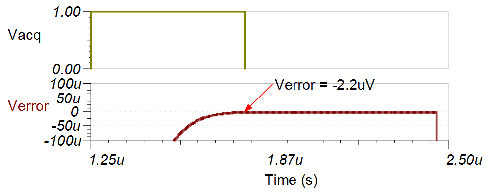
Transient ADC Input Settling Simulation
The following simulation shows settling to a –10-V DC input signal. This type of simulation shows that the sample and hold kickback filter is properly selected. See the Final SAR ADC Drive Simulations video for detailed theory on this subject. Note: in this example the amplifier had settling issues, so the sampling rate was decreased from 1MSPS to 800kSPS. Reducing the sampling rate increases the acquisition period to improve settling (tacq = 1 / fsamp – tconv = (1/800kSPS) – 710 ns = 540 ns).
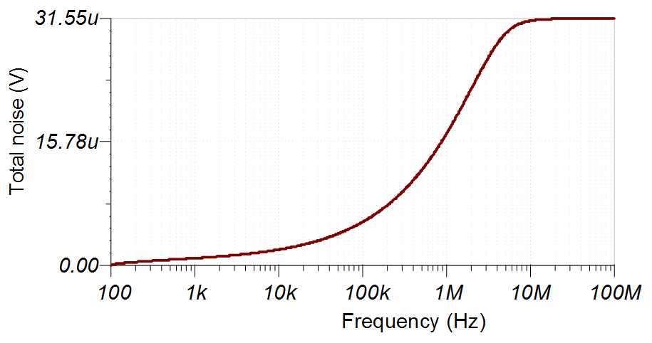
Noise Simulation
The following noise calculation takes into account the thermal noise of the resistor network, the amplifier noise, and the bandwidth limit from the filters. The calculated total noise is 29.52μV and the simulated total noise is 31.55μV. See the Op Amp Noise Calculation video for detailed theory on amplifier noise calculations, and the Calculating the Total Noise for ADC Systems video for data converter noise.
Noise equivalent input resistor network:
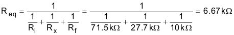
Resistor network noise:

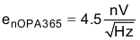
OPS365 noise density:
Noise gain:
Total noise:
Design Featured Devices and Alternative Parts
| Device | Key Features | Link | Other Possible Devices |
|---|---|---|---|
| ADS8860 | 16-bit resolution, SPI, 1-MSPS sample rate, single-ended input, Vref input range 2.5V to 5.0V | 16-bit, 1MSPS, 1-channel SAR ADC with single-ended input, SPI and daisy chain | Precision ADCs |
| OPA365 | 50-MHz bandwidth, zero crossover distortion topology, rail-to-rail input and output, noise 4.5nV/√ Hz | 2.2V, 50MHz, Low-Noise, Single-Supply Rail-to-Rail Operational Amplifier | Operational amplifiers (op amps) |
Link to Key Files
Texas Instruments, SBAA375 source files, SBAC251 software support