SBAA409A November 2019 – September 2024 ADS1018 , ADS1018-Q1 , ADS1118 , ADS1118-Q1
| Input Measurement | AINP and AINN Inputs | Digital Output ADS1118 |
|---|---|---|
| PGA[2:0] = 000, FSR = ±6.144V | 0V to 5V |
–26667 to 26667 97D5h to 682Bh |
| VDD | GND | |
|---|---|---|
| 5V | 0V | |
Design Description
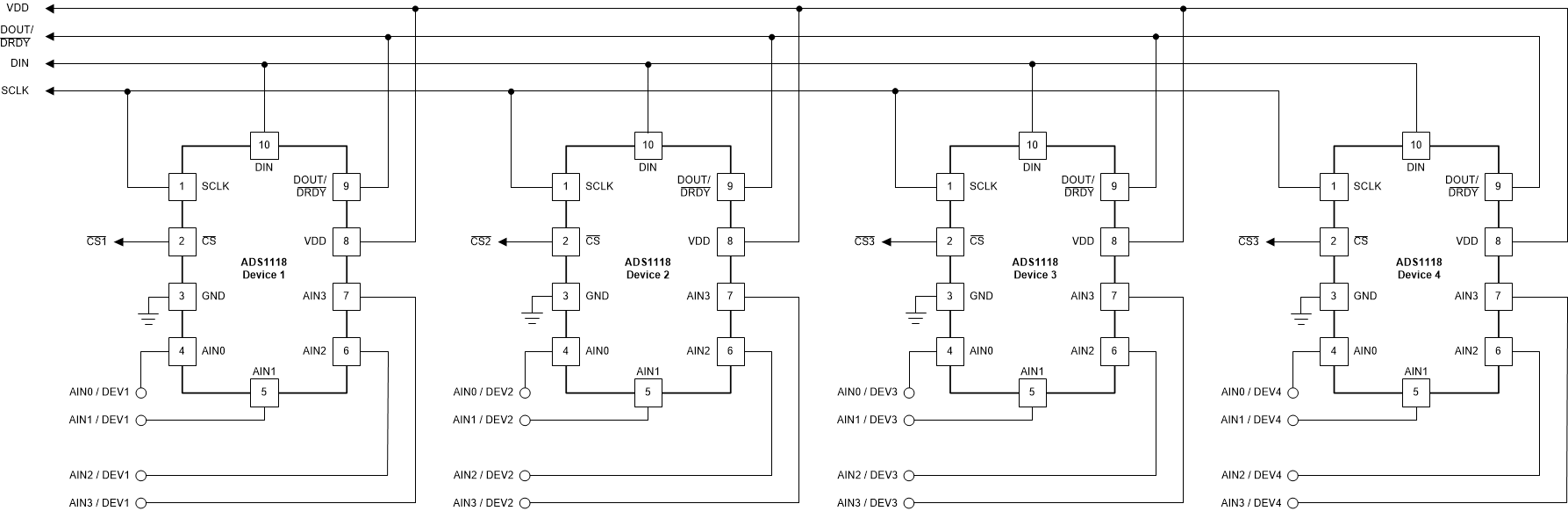
Many applications require a large array of measurements using a minimal amount of space. This circuit document describes an 8-channel measurement system using four ultra-small ADS1118 devices with Serial Peripheral Interface (SPI). These devices have an accurate internal voltage reference, and can be programmed for multiple input ranges as 16-bit differential analog-to-digital converters (ADCs). The ADCs in system are highly configurable for different data rates and voltage ranges and can even be used for alert functions. Additionally, all analog inputs can be configured individually to make a 16-channel measurement system with single-ended input measurements. The ADS1118 is available in an ultra-small 1.5mm × 2.0mm X2QFN that takes up very little space on a board. This circuit can be used in applications such as analog input modules for PLCs, lab instrumentation, and factory automation.
Design Notes
- The ADS1118 has a differential ADC. Negative measurements are made when AINN is higher than AINP and are reported in two's complement notation.
- The operating range of the ADC analog inputs is between ground and VDD, even with the full-scale range (FSR) set to voltages larger than the VDD. For example, with the FSR set to ±6.144V and VDD set to 5V, all analog inputs are limited from 0V to 5V. An FSR larger than the supply prevents over-ranging the ADC for any measurement within the operating range.
- With the internal reference, the ADS1118 device can conveniently measure its own supply using the internal reference without the need of a voltage divider.
- Use supply decoupling capacitors for the power supplies. VDD must be decoupled with at least a 0.1-μF capacitor to GND. See the ADS1118 Ultra-Small, Low-Power, SPI-Compatible, 16-Bit ADCs With Internal Reference, and Temperature Sensor data sheet for details on power-supply recommendations.
- When possible, use C0G (NPO) ceramic capacitors for input filtering. The dielectric used in these capacitors provides the most stable electrical properties over voltage, frequency, and temperature changes. Because of size, this may not always be practical and X7R capacitors are the next best alternative.
- If lower resolution is acceptable, the ADS1018 ADC may be set up in a similar system. These 12-bit ADCs allow for a faster data rate and lower cost.
- The ADS1118 device uses SPI communications. If an I2C interface is required, the ADS1115 ADC has similar functions and may be used. Additionally, the ADS1015 or the TLA2024 devices may be substituted if an ADC with less resolution can be used. See Precision measurement circuit with 16 singled-ended channels and I2C interface for more details
- This measurement system may be constructed with 16 single-ended channels instead of eight differential channels, or with different combinations of differential and single-ended channels. This system is also scalable with fewer devices and channels.
- The ADS1118 ADC is used in single-shot conversion mode. In this mode of operation, devices are enabled for each conversion and then powered down. The total power of using all four devices individually is the same as using a single device in continuous conversion.
- The ADS1118 ADC has an accurate internal temperature sensor that may also be used for an additional measurement. For more details about this measurement, see the ADS1118 data sheet.
Configuring the Device
- Setup the SPI with four CS lines to individually
select the devices.
This circuit uses four ADS1118 ADCs multiplexed to measure eight different channels. To do this, the four devices must use different CS lines, one for the CS line for each device. The remaining SPI lines (DIN, DOUT/ DRDY, and SCLK) are shared with all devices.
- Use the multiplexer to cycle through each analog input.
The ADS1118 ADC has a multiplexer for measuring multiple channels. In this design, the system cycles through each of the analog inputs of each device. While single-ended measurements are available, this system is shown by cycling through all of the analog inputs to make differential measurements.
Devices are configured through the configuration register shown in the following table. Within the configuration register, the MUX[2:0] selects the AINP and AINN nodes for the ADC and sets the input channel for each device. The settings in the following table show settings for differential measurements. As shown in the ADS1118 data sheet, single-ended measurements can be made with settings MUX[2:0] = 100 to 111.
Input Measurement ADC Input Device Input Selection Channel 1 MUX[2:0] = 000 AINP = AIN0 and AINN = AIN1 Channel 2 MUX[2:0] = 011 AINP = AIN2 and AINN = AIN3 After cycling through all four channels of the device, the system selects the next device and repeats the cycle.
- Identify the range of operation for each analog input measurement.
The ADS1118 device has an internal reference for accurate measurements and a scalable gain for the measurement. In this circuit document, the measurements shown are all differential. Negative measurements occur when AINN is higher than AINP. Single-ended measurements may be selected. However, because the ADS1118 device is a 16-bit ADC as a differential measurement, a single-ended measurement has only 15 bits of resolution.
The ADS1118 ADC can be set to one of six settings for the FSR (full-scale range). This is the equivalent to having a programmable gain amplifier on the front end of the ADC. The FSR[2:0] bits of the configuration register have settings from ±0.256V up to ±6.144V. As mentioned previously, the operating range of the ADC analog inputs is between ground and VDD, even with the FSR set to voltages larger than the VDD. For example, with the FSR set to ±6.144V and VDD set to 5V, the analog inputs are limited to 0V to 5V.
The FSR settings allow for a variety of different measurements from small voltage measurements such as temperature sensors or current shunt resistors, to larger voltage measurements ADC measuring its own supply without the need for a voltage divider. Settings for the ADS1118 FSR are shown in the following table.
Input Measurement AINN and AINP Inputs Digital Output ADS1118 PGA[2:0] = 000, FSR = ±6.144V 0V to 5V 97D5h to 682Bh PGA[2:0] = 001, FSR = ±4.096V 0V to 4.096V 8000h to 7FFFh PGA[2:0] = 010, FSR = ±2.048V 0V to 2.048V 8000h to 7FFFh PGA[2:0] = 011, FSR = ±1.024V 0V to 1.024V 8000h to 7FFFh PGA[2:0] = 100, FSR = ±0.512V 0V to 0.512V 8000h to 7FFFh PGA[2:0] = 101–111, FSR = ±0.256V 0V to 0.256V 8000h to 7FFFh As a differential measurement, the ADC reports a negative value when the AINN input is higher than the AINP input. Negative results are reported in two's complement notation.
- Set the data rate.
The ADS1118 ADC can be configured to one of eight data rates, based on the internal oscillator of the device. This data rate has a tolerance of ±10%. The data rate is set by the DR[2:0] bits shown in the following table.
Data Rate Setting Data Rate DR[2:0] = 000 8SPS DR[2:0] = 001 16SPS DR[2:0] = 010 32SPS DR[2:0] = 011 64SPS DR[2:0] = 100 128SPS DR[2:0] = 101 250SPS DR[2:0] = 110 475SPS DR[2:0] = 111 860SPS The data rate is selected to be 128SPS, which is the default setting of the ADS1118 ADC. This data rate is the fastest available that gives a noise performance better than one LSB for all FSR settings.
Configuration Register Settings
The configuration register sets the mode of operation and configuration of the ADC. Configurations include all of the settings described in the previous sections. Nine fields across 16 bits are used to configure the device. Configuration register field descriptions are shown with bit names and positions, read and write usage, and reset values in the following table.
| 15 | 14 | 13 | 12 | 11 | 10 | 9 | 8 |
|---|---|---|---|---|---|---|---|
| SS | MUX[2:0] | PGA[2:0] | MODE | ||||
| R/W-1h | R/W-0h | R/W-2h | R/W-1h | ||||
| 7 | 6 | 5 | 4 | 3 | 2 | 1 | 0 |
| DR[2:0] | TS_MODE | PULL_UP_EN | NOP[1:0] | RESERVED | |||
| R/W-4h | R/W-0h | R/W-0h | R/W-0h | R-1h | |||
The SS bit starts a single conversion. The MUX[2:0] bits set the input multiplexer to cycle through different measurements. The MODE bit sets the device to single-shot conversion mode. The DR[2:0] bits set the data rate of the device. The remaining fields are used for the ADC comparator settings which are not used in this design. See the ADS1118 Ultra-Small, Low-Power, SPI-Compatible, 16-Bit ADCs With Internal Reference, and Temperature Sensor data sheet for details on the configuration register.
As an example, one ADC is set to measure its own supply to ground, using AIN0 connected to VDD. The FSR is set to ±6.144V with a data rate of 128SPS. The following table shows the settings for the configuration register fields.
| BIT | FIELD | SETTING | DESCRIPTION |
|---|---|---|---|
| 15 | OS | 1 | Start conversion |
| 14:12 | MUX[2:0] | 000 | Differential input measurement, AINP – AINN = AIN0 – AIN1, selection of the first channel |
| 11:9 | PGA[2:0] | 000 | FSR = ±6.144V, sets the ADC to be able to measure the full supply range of 0V to VDD |
| 9 | MODE | 1 | Operation in single-shot conversion mode |
| 7:5 | DR[2:0] | 100 | Data rate = 128SPS |
| 4 | TS_MODE | 0 | Measures analog inputs instead of the temperature sensor |
| 3 | PULL_UP_EN | 0 | Disables the internal pullup resistor on the DOUT/ DRDY |
| 2:1 | NOP[1:0] | 01 | Write 01 to these bits to ensure that the device writes to the configuration register |
| 0 | RESERVED | 1 | Always write 1 to this bit |
Combining these bits from the field descriptions, the configuration register values is 1000 0001 1000 0011 or 8183h.
Channel Cycling
To cycle through each channel of the system, start each conversion, wait for the conversion to complete, and then read back the data. Then start the conversion for the next channel. Repeat each measurement for both differential input channels before moving on to the next ADC. Repeating this measurement for all four ADCs in the system cycles through all channels.
Use the associated CS line to communicate with the device. Each of the four devices has its own CS line to enable the SPI. The 32-bit data transmission cycle with configuration register read back can be used to start conversions. This communication is shown in the following figure.
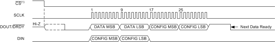
With this method, 32 SCLKs are used. Communication is full-duplex, meaning that the data is being clocked into the device at the same time as data is being clocked out of the device. The device starts a new conversion after the write of the configuration register.
As the configuration register is being written, 32 SCLKs clock out the data on DOUT/ DRDY. The first 16 bits clock out the data from the previous conversion and the second 16 bits clock out contents of the configuration register and verifies the new configuration register write.
The master then waits for the conversion to complete. For this example, the ADS1118 device is set to the default data rate of 128SPS. Because the device uses an internal oscillator, there is some variation in the data rate. To ensure that the device is read after the ADC completes a conversion, the microcontroller waits for the maximum time required for the conversion to complete. This wait time is the nominal data period plus 10% (to compensate for the internal oscillator variation of the device). An additional 20µs is added for the wake-up time of the ADC for each single-shot conversion. The total wait time is calculated in the following equation.
As an example, if the device is run at 128SPS, the nominal data period is 7.82ms. The necessary wait time is:
Instead of waiting this maximum time as previously calculated, the DOUT/ DRDY line can be monitored to read the data. When the conversion completes, the DOUT/ DRDY transitions from high to low. This transition can be used as an interrupt to indicate that the data is ready, and that it can be clocked out of the device. The 32-bit data transmission cycle makes it easier to monitor the DOUT/ DRDY. By reading back the configuration register, DOUT/ DRDY is forced high at the end of the transmission cycle. This makes it easy to find the transition from high to low. If DOUT/ DRDY is low, the data ready indication is a narrow 8-µs pulse.
Measurement Conversion
Conversions for the input voltage are based on the full-scale range (FSR) setting of the ADC. The FSR is set by the PGA[2:0] bits in the configuration register.
Negative readings are reported in two's complement notation. For example, –1 in decimal is reported as FFFFh and a negative full-scale reading is reported as 8000h.
As previously mentioned, the 16-bit ADS1118 ADC may be replaced with the 12-bit ADS1018 ADC. For these devices, the data format is 12-bits with four bits zero padded on the right. A full scale reading is 7FFh and would be read from DOUT/ DRDY as 7FF0h.
The ADS1118 device also has an onboard precision temperature sensor that can also be measured at any time. For details on the temperature conversion, see the ADS1118 data sheet.
Pseudo Code Example
The following pseudo code sequence shows the required steps to set up conversions from each channel of the four devices and collect the data after each conversion. It also includes setup for the microcontroller that interfaces to the ADC.
For each channel, the microcontroller simultaneously sets up the ADC configuration and starts the conversion. The microcontroller waits for conversion to complete, waiting enough time for the conversion and any variation in the internal oscillator frequency. Then the data is read from the conversion register. The cycle continues through each channel of each device. The setup assumes the previous configuration with the data rate set to 128SPS for the wait time for the conversion.
Configure the SPI interface of the microcontroller to SPI mode 1 (CPOL = 0, CPHA =1);
Conversions from two channels of device 1:
{
  Set CS1 to the device low;
    Send 32 SCLKs, Write 8183h, 0000h; // start conversion Channel 1, AIN0-AIN1
    Wait 8.62ms or for the DOUT/DRDY line to return low
    Send 32 SCLKs, Write B183h, 0000h; // start conversion Channel 2, AIN2-AIN3, Read Channel 1
    Wait 8.62ms or for the DOUT/DRDY line to return low
    Send 16 SCLKs; // read Channel 2
  Set CS1 to the device high;
}
Conversions from two channels of device 2:
{
  Set CS2 to the device low;
    Send 32 SCLKs, Write 8183h, 0000h; // start conversion Channel 3, AIN0-AIN1
    Wait 8.62ms or for the DOUT/DRDY line to return low
    Send 32 SCLKs, Write B183h, 0000h; // start conversion Channel 4, AIN2-AIN3, Read Channel 3
    Wait 8.62ms or for the DOUT/DRDY line to return low
    Send 16 SCLKs; // read Channel 4
  Set CS2 to the device high;
}
Conversions from two channels of device 3:
{
  Set CS3 to the device low;
    Send 32 SCLKs, Write 8183h, 0000h; // start conversion Channel 5, AIN0-AIN1
    Wait 8.62ms or for the DOUT/DRDY line to return low
    Send 32 SCLKs, Write B183h, 0000h; // start conversion Channel 6, AIN2-AIN3, Read Channel 5
    Wait 8.62ms or for the DOUT/DRDY line to return low
    Send 16 SCLKs; // read Channel 6
  Set CS3 to the device high;
}
Conversions from two channels of device 4:
{
  Set CS4 to the device low;
    Send 32 SCLKs, Write 8183h, 0000h; // start conversion Channel 7, AIN0-AIN1
    Wait 8.62ms or for the DOUT/DRDY line to return low
    Send 32 SCLKs, Write B183h, 0000h; // start conversion Channel 8, AIN2-AIN3, Read Channel 7
    Wait 8.62ms or for the DOUT/DRDY line to return low
    Send 16 SCLKs; // read Channel 8
  Set CS4 to the device high;
}
Layout Example
The following image shows an example layout of one of the four ADS1118 devices. Differential RC input filtering is added using 0402 resistors and capacitors. The resulting layout is about 280 mils by 340 mils.
 Example
Layout
Example
LayoutDesign Featured Devices
| Device | Key Features | Link | Other Possible Devices |
|---|---|---|---|
| ADS1118 | ADS1118 ultra-small, low-power, SPI-compatible, 16-bit ADCs with internal reference, oscillator, and temperature sensor | 16-bit, 860-SPS, 4-channel, delta-sigma ADC with PGA, oscillator, VREF, temp sensor and SPI |