SBAA506 March 2021 ADS131B04-Q1 , ADS131M02 , ADS131M03 , ADS131M04 , ADS131M06 , ADS131M08
Design Description
This circuit shows an external solution to protect ADS131M02, ADS131M03, ADS131M04, ADS131M06, and ADS131M08 Delta-Sigma ADCs from electrical overstress (EOS). The protection is implemented with external Schottky diodes and switching diodes. This document shows how the Schottky diodes and switching diodes can be used with current-limiting resistors to implement the external protection clamp for the overstress signal and maintain a minimum impact on performance, especially signal-to-noise ratio (SNR) and total harmonic distortion (THD). This circuit is useful in the following end equipment: Battery test, Semiconductor test, Electricity meter, Power quality analyzer, and Power quality meter. For protecting high-voltage SAR ADCs from electrical overstress, see Input protection for high-voltage ADC circuit with TVS diode and Circuit for protecting ADC with TVS diode and PTC fuse. For protecting low-voltage SAR ADC from electrical overstress, see Circuit for protecting low-voltage SAR ADCs from electrical overstress with minimal impact on performance.
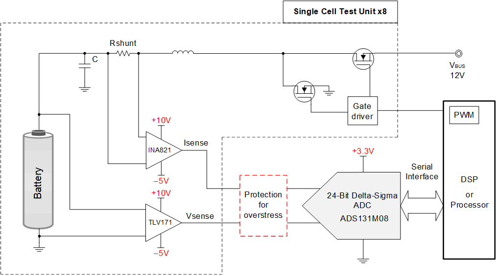
The following figure comes from the Digital Control Reference Design for Cost-Optimized Battery Test Systems Reference Design in the Battery Test application. During an electrical overstress event, this circuit can potentially apply damaging voltages and currents to the inputs of the ADS131M08 ADC: the voltage from the amplifiers (INA821 and TLV171) can reach the power supply voltages (+10V or –5V), and the overstress current from the amplifiers can be as high as the short-circuit current for each respective amplifier.