-
Understanding and Using SAR ADC SPICE Micromodel
- Trademarks
- 1Introduction
-
2
Internal Topology of SAR ADC Model
- 2.1 Sample and Hold
- 2.2 Sample and Hold Timing
- 2.3 Reference Transients
- 2.4 Bandwidth Modeling
- 2.5 Noise Modeling
- 2.6 Reference Droop and Reference Noise Errors
- 2.7 Gain, Offset, and Input Leakage Modeling
- 2.8 Differential input behavior
- 2.9 ESD Protection Diodes and Parasitic Capacitance
- 2.10 Summary of Parameters
- 2.11 Summary of Model Pins
- 3Downloading and Using PSpice® Example Projects From Web
- 4Summary
- IMPORTANT NOTICE
Understanding and Using SAR ADC SPICE Micromodel
Trademarks
PSpice is a registered trademark of Cadence Design Systems, Inc..
All trademarks are the property of their respective owners.
1 Introduction
This document describes the operation and design of a flexible Successive Approximation Register (SAR) Analog to Digital Converter (ADC) model. The model was developed to be easily modifiable using SPICE parameters so that it can be used for simulating the behavior of many different SAR ADCs. By adjusting the parameters, this behavioral model can be modified to cover many different models of SAR ADCs. This document defines each parameter and shows how the parameter value can be determined from the device data sheet. Thus, if a model for a particular device is not available, the general model can be modified to cover most ADCs. Figure 1-1 shows the spice model with its associated parameter list. Various performance criteria such as input switching transients, noise, and offset can be modified by adjusting the model parameters. The first part of this document covers the internal operation of the model and how the external parameters can be set using data sheet criteria. The second part of this document covers ADC design optimization using the model. The final part of this document covers design performance verification using the model.
 Figure 1-1 ADC Model With Parameters
2 Internal Topology of SAR ADC Model
This section provides a simplified description of the internal operation of the model. Also, the meaning of the external parameters and selection of values based on data sheet criteria are covered.
2.1 Sample and Hold
A SAR ADC operates by sampling the input signal during the acquisition period and holding the signal during the conversion period. The sampling action is performed during the acquisition period by closing switch SW1 and allowing sampling Csh to charge via resistor Rsh. At the end of the acquisition period, the switch is opened and the input voltage is held for conversion. To achieve minimal distortion, the capacitor Csh needs to be fully settled at the end of the acquisition phase to properly measure the externally applied signal. The settling is dependent on amplifier bandwidth, the external RC filter, the internal sampling circuit, and the ADC timing. The model has a Vsamp output that shows the sampling behavior, and a Vsettling_error output that displays the difference between the sampled value and the steady state input signal. This settling analysis can be used to facilitate the selection of the amplifier and optimization of the external RC circuit. An input drive circuit optimization is covered in detail in Section 3.1. Figure 2-1 illustrates the ADC system design with the internal sample and hold circuit. Note that Rsh and Csh are parameters that can be adjusted according to the ADC data sheet. Most SAR ADC data sheets provide an input sampling stage equivalent circuit. This circuit provides values for Rsh and Csh.
 Figure 2-1 ADC System Showing External
Drive Circuit and Internal Sample and Hold
Figure 2-1 ADC System Showing External
Drive Circuit and Internal Sample and Hold2.2 Sample and Hold Timing
As previously mentioned, the conversion cycle is broken into an acquisition phase where the sample and hold switch is closed and a conversion phase where the switch is opened and the sampled signal is held. The conversion period is a fixed amount of time set by an internal oscillator or external clock signal. Most converters transition to the acquisition period whenever the ADC is not converting. For example, assume the converter has a conversion phase (TCONV) that lasts for 710 ns. If the device sampling rate is 1 Msps, or 1 sample/µs, then the acquisition period can be calculated by subtracting the conversion phase from the device throughput (tacq = throughput – TCONV= 1 µs – 710 ns = 290 ns). Furthermore, if the sampling rate is reduced to 100 ksps, the conversion period remains the same and the acquisition period naturally gets longer (tacq = 10 µs – 710 ns = 9.29 µs ).
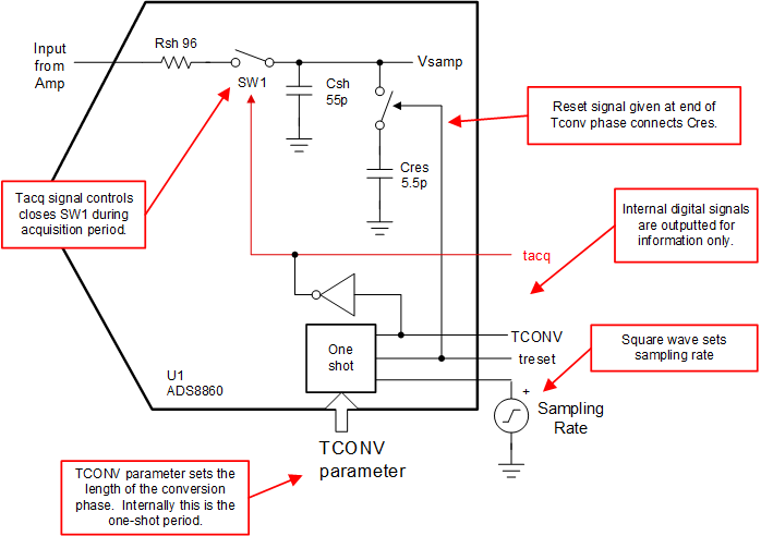
The model includes a parameter to set TCONV, and uses an external square wave to set the sampling rate. The external square wave triggers an internal one-shot timer that initiates the conversion phase. The conversion phase lasts for a time specified by the parameter TCONV. Inside the model the parameter TCONVis used to set the timing capacitor for the one-shot. Whenever the device is not converting it is acquiring, so the tacq signal is the inversion of TCONV.
The TCONVand tacq signals are used to control the timing of the sample and hold circuit. The sample and hold switch is closed throughout the tacq period and open during the TCONV period. At the end of the TCONVperiod a small reset sample and hold signal is generated. This signal connects Csh in parallel with a reset capacitor. The reset capacitor initially charged to 0 V, so when it is connected in parallel with Csh it causes the voltage on Csh to droop. This droop emulates the real-world behavior of a sample and hold circuit. The droop happens as a result of the conversion process and typically it is about 10% of the held voltage. Thus, Creset is typically sized to be 10% of Csh. Figure 2-2 below shows the sample and hold timing control.
 Figure 2-2 Sample and Hold Timing Control