SBAA531 November 2021 ADS8860 , ADS8862 , ADS8881 , ADS9110 , ADS9224R
- Trademarks
- 1Introduction
-
2
Internal Topology of SAR ADC Model
- 2.1 Sample and Hold
- 2.2 Sample and Hold Timing
- 2.3 Reference Transients
- 2.4 Bandwidth Modeling
- 2.5 Noise Modeling
- 2.6 Reference Droop and Reference Noise Errors
- 2.7 Gain, Offset, and Input Leakage Modeling
- 2.8 Differential input behavior
- 2.9 ESD Protection Diodes and Parasitic Capacitance
- 2.10 Summary of Parameters
- 2.11 Summary of Model Pins
- 3Downloading and Using PSpice® Example Projects From Web
- 4Summary
2.5 Noise Modeling
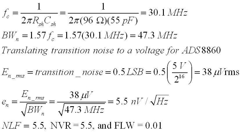
The noise for the ADC is primarily from the switch resistance in the sample and hold circuit Rsh. However, there are secondary noise sources that are not accounted for by Rsh which can make a significant difference in the total noise simulation. To model noise as accurately as possible, noise is defined by a noise source and internal resistors are all noiseless. The noise signal source is adjustable via the external parameter list. Noise parameters are: NLF, FLW, and NVR. NLF is the noise in the flicker region. FLW is the frequency that the flicker noise is specified at. NVR is the noise in the broadband region. For most ADC models the flicker noise is not specified, so NLF and NVR are set to the same value and FLW is set to an arbitrary low value such as 0.01. NLF and NVR are given in nV/√Hz. For example, setting NLF = 10, NVR = 10, and FLW = 0.01 indicates that noise density is flat and is equal to 10 nV/√Hz. Figure 2-6 shows the noise model for the ADC.
 Figure 2-6 ADC Noise Model
Typically, the ADC data sheet specifies noise as a total RMS noise. This may be done directly as a transition noise, or indirectly in the SNR specification. To choose the correct value for the noise parameters, convert the total RMS noise into a noise density. Figure 2-7 shows that calculation. Note that the models in the TI library already have this parameter adjusted as needed. This procedure is only needed when a new model is being developed. Review Calculating ADC Noise Video for details on the calculations.
 Figure 2-7 Selecting the Noise Parameters