SBAA645 October 2024 AMC0311R-Q1 , AMC0330R-Q1
2.2 Isolated Amplifiers With Single-Ended, Fixed-Gain Output
The new product family offers alternative devices for compact designs that do not benefit from the differential output. The differences between a differential and single-ended output amplifier can be summarized primarily by how these amplifiers handle noise, output signals, and the design characteristics. The new device family introduces two options of single-ended amplifiers: the single-ended amplifier with fixed gain and the single-ended amplifier with ratiometric gain.
The single-ended fixed gain amplifier is widely desired due to the ease of use and cost-effectiveness. The single ended fixed gain amplifier can output a single-ended signal that is proportional to the input voltage of the amplifier. As this device was designed to interface directly with a single-ended input ADC, the additional differential to single-ended amplifier conversion stage, as previously referenced in Figure 2-1, is no longer necessary. Therefore, this design requires less components which enables a smaller design size and lower BOM cost, making this device designed for compact systems.
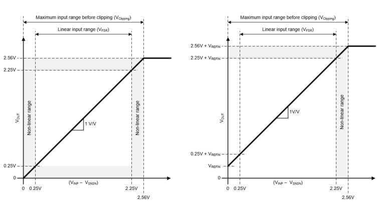
One design consideration for the single-ended fixed gain devices is the device's ground noise sensitivity. Fluctuations to the ground potential can bring distortions to the output signal by introducing noise or error to the signal, which can be eliminated with proper grounding and component selection. If not considered, this can potentially decrease your signal to noise ratio and decrease overall performance. Another design consideration is the voltage applied to the reference (REFIN) pin of the device - the pinout of the device is shown in Figure 2-4 . Figure 2-2 shows the input-to-output transfer characteristic for the AMC0x11S device, which is the single-ended fixed gain output device that has an input voltage range of 0-2.25V.
 Figure 2-2 Input-to-output Transfer Characteristic for AMC0x11S
The left image shows the case in which REFIN is shorted to GND2. The right image shows when VREFIN = 250mV. Supplying a voltage to REFIN that is ≥250mV extends the linear input voltage range to 0V. The output buffer requires a minimum headroom of 250mV for linear operation. Therefore, with REFIN shorted to GND2, the device shows non-linear behavior for input voltages near 0V. The equation for the output voltage of AMC0x11S device is:
Output Voltage of AMC0x11S:
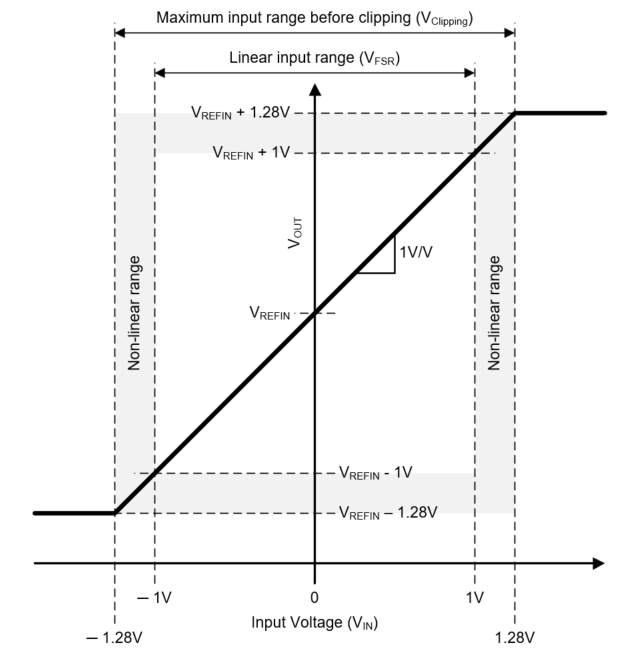
For the AMC0x30S device, which is the single-ended, fixed gain device that has an input voltage range of ±1V, the output is directly proportional to the input voltage (VIN), where REFIN is referred to GND2. The output can be defined by the following equation:
Output Voltage of AMC0x30S:
Figure 2-3 shows the input-to-output transfer characteristic for the AMC0x30S device. For input voltages below –1V and above +1V, the output of the device continues to follow the input but with reduced linearity performance.
 Figure 2-3 Input-to-output Transfer Characteristic for AMC0x30S