SBAA645 October 2024 AMC0311R-Q1 , AMC0330R-Q1
2.3 Isolated Amplifiers With Single-Ended, Ratiometric Output
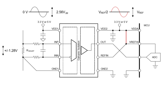
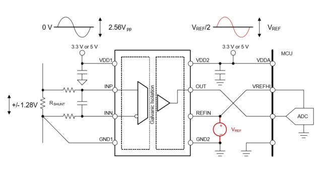
To provide a comprehensive portfolio of devices that covers the need for high performance, cost-efficient, and smaller system sizes, the new product family includes options of single-ended devices with a ratiometric output. The single-ended ratiometric output devices of the new product family are designed to adjust the gain in proportion to the reference voltage of the ADC. One disadvantage of the fixed gain output is that the fixed gain can only provide a 2V output swing. Systems with a 5V analog IO can only use 50% of the ADC input range, therefore losing 1 bit of resolution on the measurement. The ratiometric output makes sure that the amplifier fully utilizes the ADC dynamic range, thereby maximizing the resolution of the measurement. Figure 2-4 and Figure 2-5 refer to two different configurations for the ratiometric devices:
 Figure 2-4 REF Derived from Supply
 Figure 2-5 REF Supplied by External Reference
Having the reference voltage derived from the power supply rail can contribute to lower costs, as there can be less components involved. However, having the reference voltage derived from an external reference can lead to lower noise.
The design of the single-ended ratiometric output device makes the device insensitive to the value of the reference voltage and tolerant of inaccuracy and AC disturbance. Because of the device's ability to achieve increased resolution, accuracy and stability while eliminating the need for the additional differential to single-ended amplifier stage, the ratiometric option is desired greatly for the cost savings and ability to take up less PCB space and contribute to lower BOM cost, all while meeting performance specifications.
One design consideration for the single-ended, ratiometric device is the input voltage range of the ADC. Because the ratiometric devices can support 2.75-5.5V reference voltages, the ratiometric devices are best designed for ADC with an input voltage range of 3.3V and 5V. Another design consideration for this device is routing. Because the reference voltage of both the ADC and the amplifier are proportional, the reference voltage of the ADC needs to be routed to the ratiometric device.
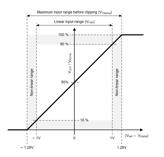
Figure 2-6 shows the input-to-output transfer characteristics for the AMC0x30R, which is the single-ended, ratiometric gain device that has an input voltage range of ±1V. The bipolar input device can output 50% of VREF at VIN = 0 due to the amplifier being biased around the midpoint of the reference voltage
 Figure 2-6 Input-to-Output Transfer Characteristic for
AMC0x30R
Figure 2-6 Input-to-Output Transfer Characteristic for
AMC0x30RFor any input voltage within the specified linear input range, the device outputs a voltage can be defined by the following equation:
Output Voltage of AMC0x30R:
For input voltages below –1V and above +1V, the output of device continues to follow the input but with reduced linearity performance.
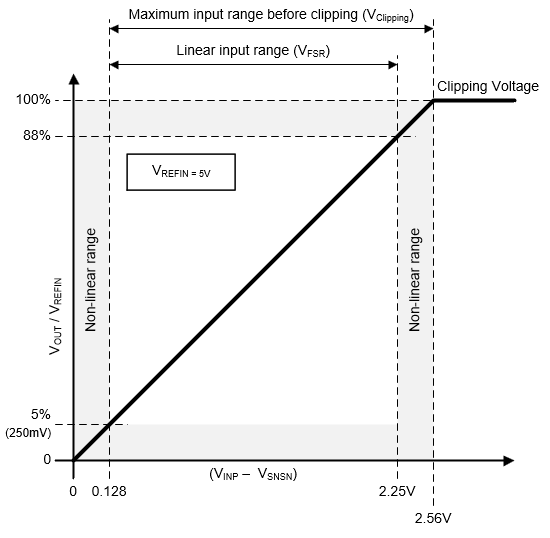
The AMC0x11R, which is the single-ended, ratiometric device that has an input voltage range of 0.13-2.25V, has an output voltage that is defined by the following equation:
Output Voltage of AMC0x11R:
Similar to the AMC0x11S, the AMC0x11R device shows non-linear behavior for input voltages near 0V, is shown in Figure 2-7.
 Figure 2-7 Input-to-Output Transfer Characteristic for
AMC0x11R
Figure 2-7 Input-to-Output Transfer Characteristic for
AMC0x11RAt VREFIN=5V, the minimum input voltage for linear operation is 128mV. The output is 5% of the reference, or 250mV.
The minimum input voltage for linear operation can be calculated using the following equation:
Minimum Input Voltage for Linear Operation for AMC0x11R: