SBAA645 October 2024 AMC0311R-Q1 , AMC0330R-Q1
2.1 Isolated Amplifiers with Differential Output
Differential output amplifiers are widely desired in systems requiring high accuracy, noise immunity, and designed for signal integrity. The differential output amplifier provides two outputs: a positive and a negative output that are equal in magnitudes but opposite in phase. With two equally balanced output signals, the differential output amplifier has the ability to handle ground shifts without signal degradation, making the differential output amplifier designed for high-precision and performance applications. Because of the amplifier's insensitivity to ground shifts, these devices enable routing for the output signal over long distances while still maintaining signal integrity.
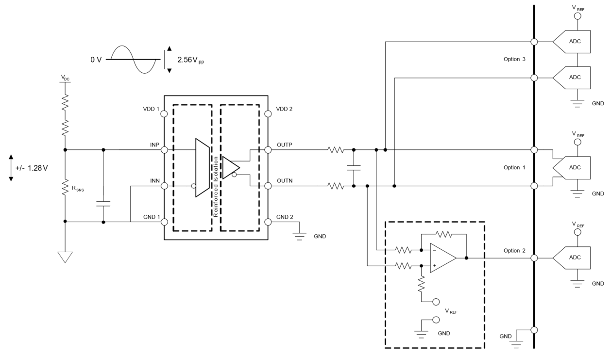
There are a few design considerations with a differential output amplifier. One of these considerations is PCB layout. Having poor PCB layout can compromise the amplifier’s ability to maintain an accurate common-mode output voltage. Since differential amplifiers rely on both the inverting and non-inverting paths, maintaining symmetry by making sure equal PCB trace lengths for both output lines is essential for minimizing output errors. There are different design options for configuring the differential output amplifier to an analog-to-digital converter (ADC). Option one, as shown in Figure 2-1, is a configuration that directly interfaces the differential output amplifier to a differential input ADC. However, processors such as the MSP430 and the C2000 have embedded single-ended input ADC. This consideration creates the need to convert from the differential signal to a single-ended signal to interface directly with the ADC. The best design for outputting to single-ended input ADC has been the conversion of the differential to single-ended output, as shown as Option 2 in Figure 2-1.
 Figure 2-1 Differential Output Configuration
This configuration introduces an additional amplifier, which allows for the conversion of a differential signal to a single-ended signal that outputs directly to the ADC. For more information about interfacing a differential to single-ended output stage, see, Isolated Current-Sensing Circuit With ±250-mV Input Range and Single-Ended Output Voltage, analog engineer's circuit. Another design is using two single-ended input ADC and subtracting the values in the MCU, as shown as Option 3 in Figure 2-1. However, Option 3 has the drawback of compound error and the need for an extra ADC, which makes this option less attractive.