-
DAC8x11 2-V to 5.5-V, 80-μA, 14- and 16-Bit, Low-Power, Single-Channel, Digital-to-Analog Converters in SC70 Package
- 1 Features
- 2 Applications
- 3 Description
- 4 Revision History
- 5 Device Comparison
- 6 Pin Configuration and Functions
- 7 Specifications
- 8 Detailed Description
- 9 Application and Implementation
- 10Power Supply Recommendations
- 11Layout
- 12Device and Documentation Support
- 13Mechanical, Packaging, and Orderable Information
- IMPORTANT NOTICE
DAC8x11 2-V to 5.5-V, 80-μA, 14- and 16-Bit, Low-Power, Single-Channel, Digital-to-Analog Converters in SC70 Package
1 Features
- Relative Accuracy:
- 1 LSB INL (DAC8311: 14-bit)
- 4 LSB INL (DAC8411: 16-bit)
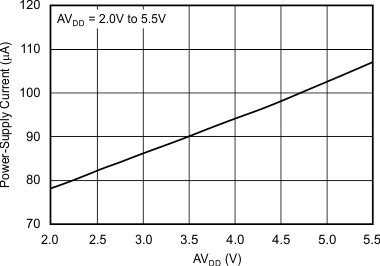
- microPower Operation: 80 μA at 2 V
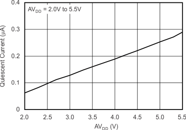
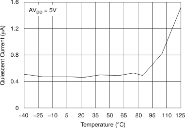
- Power-Down: 0.5 μA at 5 V, 0.1 μA at 2 V
- Wide Power Supply: 2 V to 5.5 V
- Power-On Reset to Zero Scale
- Straight Binary Data Format
- Low Power Serial Interface With Schmitt-Triggered Inputs: Up to 50 MHz
- On-Chip Output Buffer Amplifier, Rail-to-Rail Operation
- SYNC Interrupt Facility
- Extended Temperature Range –40°C to 125°C
- Pin-Compatible Family in a Tiny, 6-Pin SC70 Package
2 Applications
- Portable, Battery-Powered instruments
- Process Controls
- Digital Gain and Offset Adjustment
- Programmable Voltage and Current Sources
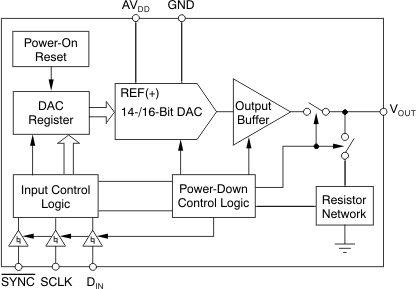
Simplified Schematic
3 Description
The DAC8311 (14-bit) and DAC8411 (16-bit) devices are low-power, single-channel, voltage output digital-to-analog converters (DAC). They provide excellent linearity and minimize undesired code-to-code transient voltages while offering an easy upgrade path within a pin-compatible family. All devices use a versatile, 3-wire serial interface that operates at clock rates of up to 50 MHz and is compatible with standard SPI™, QSPI™, Microwire, and digital signal processor (DSP) interfaces.
All devices use an external power supply as a reference voltage to set the output range. The devices incorporate a power-on reset (POR) circuit that ensures the DAC output powers up at 0 V and remains there until a valid write to the device occurs. The DAC8311 and DAC8411 contain a power-down feature, accessed over the serial interface, that reduces current consumption of the device to 0.1 μA at 2 V in power down mode. The low power consumption of these devices in normal operation makes it ideally suited for portable, battery-operated equipment. The power consumption is 0.55 mW at 5 V, reducing to 2.5 μW in power-down mode.
These devices are pin-compatible with the DAC5311, DAC6311, and DAC7311, offering an easy upgrade path from 8-, 10-, and 12-bit resolution to 14- and 16-bit. All devices are available in a small, 6-pin, SC70 package. This package offers a flexible, pin-compatible, and functionally-compatible drop-in solution within the family over an extended temperature range of –40°C to 125°C.
Device Information(1)
| PART NUMBER | PACKAGE | BODY SIZE (NOM) |
|---|---|---|
| DAC8311 DAC8411 |
SC70 (6) | 2.00 mm × 1.25 mm |
- For all available packages, see the orderable addendum at the end of the data sheet.
4 Revision History
Changes from B Revision (May 2013) to C Revision
- Added ESD Ratings table, Feature Description section, Device Functional Modes, Application and Implementation section, Power Supply Recommendations section, Layout section, Device and Documentation Support section, and Mechanical, Packaging, and Orderable Information section Go
Changes from A Revision (August, 2011) to B Revision
- Changed all 1.8V to 2.0V throughout data sheetGo
- Deleted 1.8-V Typical Characteristics sectionGo
- Changed X-axis for Figure 35Go
- Changed X-axis for Figure 36Go
Changes from * Revision (August, 2008) to A Revision
6 Pin Configuration and Functions
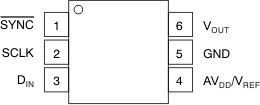
Pin Functions
| PIN | I/O | DESCRIPTION | |
|---|---|---|---|
| NAME | NO. | ||
| AVDD/VREF | 4 | I | Power Supply Input, +2 V to +5.5 V. |
| DIN | 3 | I | Serial Data Input. Data is clocked into the 24-bit (DAC8411) or 16-bit (DAC8311) input shift register on the falling edge of the serial clock input. |
| GND | 5 | — | Ground reference point for all circuitry on the part. |
| SCLK | 2 | I | Serial Clock Input. Data can be transferred at rates up to 50 MHz. |
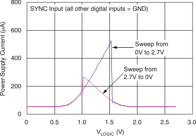
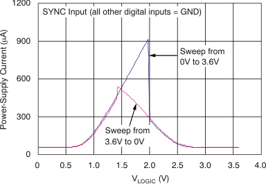
| SYNC | 1 | I | Level-triggered control input (active low). This is the frame sychronization signal for the input data. When SYNC goes low, it enables the input shift register and data are transferred in on the falling edges of the following clocks. The DAC is updated following the 24th (DAC8411) or 16th (DAC8311) clock cycle, unless SYNC is taken high before this edge, in which case the rising edge of SYNC acts as an interrupt and the write sequence is ignored by the DAC8x11. Refer to the DAC8311 and DAC8411SYNC Interrupt sections for more details. |
| VOUT | 6 | O | Analog output voltage from DAC. The output amplifier has rail-to-rail operation. |
7 Specifications
7.1 Absolute Maximum Ratings
over operating free-air temperature range (unless otherwise noted)(1)| MIN | MAX | UNIT | ||||
|---|---|---|---|---|---|---|
| Voltage | AVDD to GND | –0.3 | 6 | V | ||
| Digital input voltage to GND | –0.3 | AVDD +0.3 | V | |||
| VOUT to GND | –0.3 | AVDD +0.3 | V | |||
| Temperature | Junction, TJ max | 150 | °C | |||
| Storage, Tstg | –65 | 150 | °C | |||
7.2 ESD Ratings
| VALUE | UNIT | |||
|---|---|---|---|---|
| V(ESD) | Electrostatic discharge | Human-body model (HBM), per ANSI/ESDA/JEDEC JS-001(1) | ±1000 | V |
| Charged-device model (CDM), per JEDEC specification JESD22-C101(2) | ±500 | |||
7.3 Recommended Operating Conditions
over operating free-air temperature range (unless otherwise noted)| MIN | NOM | MAX | UNIT | ||
|---|---|---|---|---|---|
| TA | Operating temperature | –40 | +125 | °C | |
| AVDD | Supply voltage | 2.0 | +5.5 | V | |
7.4 Thermal Information
| THERMAL METRIC(1) | DAC8x11 | UNIT | |
|---|---|---|---|
| DCK (SC70) | |||
| 6 PINS | |||
| RθJA | Junction-to-ambient thermal resistance | 216.4 | °C/W |
| RθJC(top) | Junction-to-case (top) thermal resistance | 52.1 | °C/W |
| RθJB | Junction-to-board thermal resistance | 65.9 | °C/W |
| ψJT | Junction-to-top characterization parameter | 1.3 | °C/W |
| ψJB | Junction-to-board characterization parameter | 65.2 | °C/W |
| RθJC(bot) | Junction-to-case (bottom) thermal resistance | N/A | °C/W |
7.5 Electrical Characteristics
at AVDD = 2 V to 5.5 V, RL = 2 kΩ to GND, and CL = 200 pF to GND, and TA = –40°C to +125°C unless otherwise noted.| PARAMETER | TEST CONDITIONS | DAC8411, DAC8311 | UNIT | ||||
|---|---|---|---|---|---|---|---|
| MIN | TYP | MAX | |||||
| STATIC PERFORMANCE(1) | |||||||
| DAC8411 | Resolution | 16 | Bits | ||||
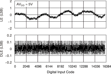
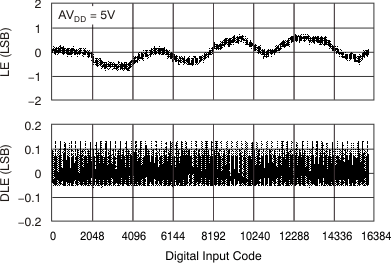
| Relative accuracy | Measured by the line passing through codes 485 and 64714 | 3.6 V to 5 V | ±4 | ±8 | LSB | ||
| 2 V to 3.6 V | ±4 | ±12 | |||||
| Differential nonlinearity | ±0.5 | ±2 | LSB | ||||
| DAC8311 | Resolution | 14 | Bits | ||||
| Relative accuracy | Measured by the line passing through codes 120 and 16200 | ±1 | ±4 | LSB | |||
| Differential nonlinearity | ±0.125 | ±1 | LSB | ||||
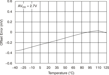
| Offset error | Measured by the line passing through two codes(2) | ±0.05 | ±4 | mV | |||
| Offset error drift | 3 | μV/°C | |||||
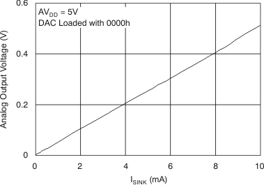
| Zero code error | All zeros loaded to the DAC register | 0.2 | mV | ||||
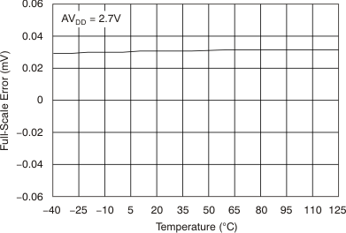
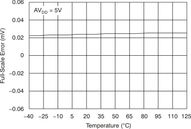
| Full-scale error | All ones loaded to DAC register | 0.04 | 0.2 | % of FSR | |||
| Gain error | 0.05 | ±0.15 | % of FSR | ||||
| Gain temperature coefficient | AVDD = 5 V | ±0.5 | ppm of FSR/°C | ||||
| AVDD = 2 V | ±1.5 | ||||||
| OUTPUT CHARACTERISTICS | |||||||
| Output voltage range | 0 | AVDD | V | ||||
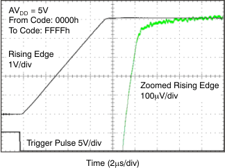
| Output voltage settling time(3) | RL = 2 kΩ, CL = 200 pF, AVDD = 5 V, 1/4 scale to 3/4 scale |
6 | 10 | μs | |||
|
RL = 2 MΩ, CL = 470 pF |
12 | μs | |||||
| Slew rate | 0.7 | V/μs | |||||
| Capacitive load stability | RL = ∞ | 470 | pF | ||||
| RL = 2 kΩ | 1000 | pF | |||||
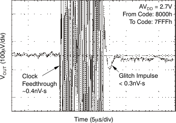
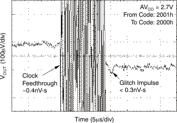
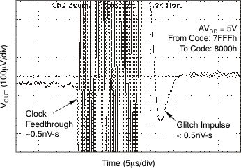
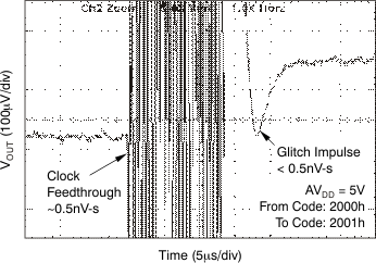
| Code change glitch impulse | 1LSB change around major carry | 0.5 | nV-s | ||||
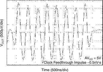
| Digital feedthrough | 0.5 | nV-s | |||||
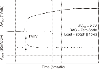
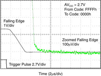
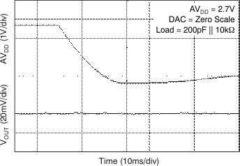
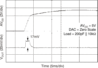
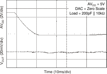
| Power-on glitch impulse | RL = 2 kΩ, CL = 200 pF, AVDD = 5 V | 17 | mV | ||||
| DC output impedance | 0.5 | Ω | |||||
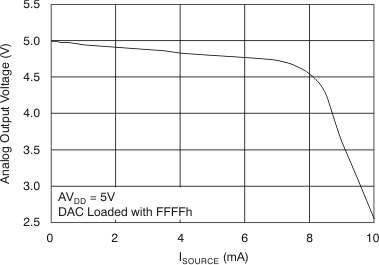
| Short-circuit current | AVDD = 5 V | 50 | mA | ||||
| AVDD = 3 V | 20 | mA | |||||
| Power-up time | Coming out of power-down mode | 50 | μs | ||||
| AC PERFORMANCE | |||||||
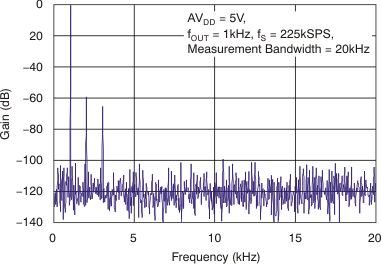
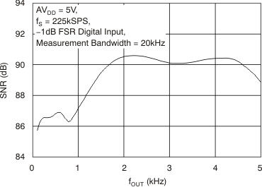
| SNR | TA= 25°C, BW = 20 kHz, 16-bit level, AVDD = 5 V, fOUT = 1 kHz, 1st 19 harmonics removed for SNR calculation |
88 | dB | ||||
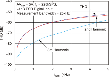
| THD | –66 | dB | |||||
| SFDR | 66 | dB | |||||
| SINAD | 66 | dB | |||||
| DAC output noise density(4) | TA= 25°C, at zero-scale input, fOUT = 1 kHz, AVDD = 5 V |
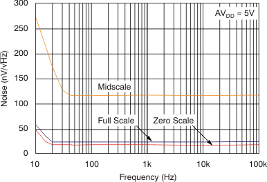
17 | nV/√Hz | ||||
| TA= 25°C, at mid-code input, fOUT = 1 kHz, AVDD = 5 V |
110 | nV/√Hz | |||||
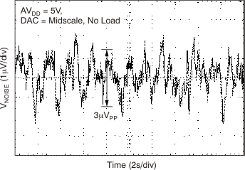
| DAC output noise(5) | TA= 25°C, at mid-code input, 0.1 Hz to 10 Hz, AVDD = 5 V |
3 | μVpp | ||||
| LOGIC INPUTS(3) | |||||||
| Input current | ±1 | μA | |||||
| VINL, input low voltage | AVDD = 2.7 V to 5.5 V | 0.3 × AVDD | V | ||||
| AVDD = 2 V to 2.7 V | 0.1 × AVDD | V | |||||
| VINH, input high voltage | AVDD = 2.7 V to 5.5 V | 0.7 × AVDD | V | ||||
| AVDD = 2 V to 2.7 V | 0.9 × AVDD | V | |||||
| Pin capacitance | 1.5 | 3 | pF | ||||
| POWER REQUIREMENTS | |||||||
| AVDD | 2 | 5.5 | V | ||||
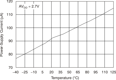
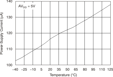
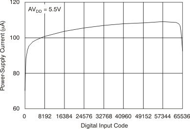
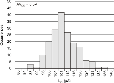
| IDD | Normal mode | VINH = AVDD and VINL = GND, at mid-scale code(6) | AVDD = 3.6 V to 5.5 V | 110 | 160 | μA | |
| AVDD = 2.7 V to 3.6 V | 95 | 150 | |||||
| AVDD = 2 V to 2.7 V | 80 | 140 | |||||
| All power-down mode | VINH = AVDD and VINL = GND, at mid-scale code(6) | AVDD = 3.6 V to 5.5 V | 0.5 | 3.5 | μA | ||
| AVDD = 2.7 V to 3.6 V | 0.4 | 3.0 | |||||
| AVDD = 2 V to 2.7 V | 0.1 | 2.0 | |||||
| Power dissipation | Normal mode | VINH = AVDD and VINL = GND, at mid-scale code(6) | AVDD = 3.6 V to 5.5 V | 0.55 | 0.88 | mW | |
| AVDD = 2.7 V to 3.6 V | 0.25 | 0.54 | |||||
| AVDD = 2 V to 2.7 V | 0.14 | 0.38 | |||||
| All power-down mode | VINH = AVDD and VINL = GND, at mid-scale code(6) | AVDD = 3.6 V to 5.5 V | 2.50 | 19.2 | μW | ||
| AVDD = 2.7 V to 3.6 V | 1.08 | 10.8 | |||||
| AVDD = 2 V to 2.7 V | 0.72 | 8.1 | |||||
7.6 Timing Requirements: 14-Bit
All specifications at –40°C to 125°C, and AVDD = 2 V to 5.5 V, unless otherwise noted.(1)(2)| PARAMETER | TEST CONDITIONS | MIN | TYP | MAX | UNIT | |
|---|---|---|---|---|---|---|
| f(SCLK) | Serial clock frequency | AVDD = 2.0 V to 3.6 V | 20 | MHz | ||
| AVDD = 3.6 V to 5.5 V | 50 | |||||
| t1 | SCLK cycle time | AVDD = 2 V to 3.6 V | 50 | ns | ||
| AVDD = 3.6 V to 5.5 V | 20 | |||||
| t2 | SCLK high time | AVDD = 2 V to 3.6 V | 25 | ns | ||
| AVDD = 3.6 V to 5.5 V | 10 | |||||
| t3 | SCLK low time | AVDD = 2 V to 3.6 V | 25 | ns | ||
| AVDD = 3.6 V to 5.5 V | 10 | |||||
| t4 | SYNC to SCLK rising edge setup time | AVDD = 2 V to 3.6 V | 0 | ns | ||
| AVDD = 3.6 V to 5.5 V | 0 | |||||
| t5 | Data setup time | AVDD = 2 V to 3.6 V | 5 | ns | ||
| AVDD = 3.6 V to 5.5 V | 5 | |||||
| t6 | Data hold time | AVDD = 2 V to 3.6 V | 4.5 | ns | ||
| AVDD = 3.6 V to 5.5 V | 4.5 | |||||
| t7 | SCLK falling edge to SYNC rising edge | AVDD = 2 V to 3.6 V | 0 | ns | ||
| AVDD = 3.6 V to 5.5 V | 0 | |||||
| t8 | Minimum SYNC high time | AVDD = 2 V to 3.6 V | 50 | ns | ||
| AVDD = 3.6 V to 5.5 V | 20 | |||||
| t9 | 16th SCLK falling edge to SYNC falling edge | AVDD = 2 V to 3.6 V | 100 | ns | ||
| AVDD = 3.6 V to 5.5 V | 100 | |||||
| t10 | SYNC rising edge to 16th SCLK falling edge (for successful SYNC interrupt) |
AVDD = 2 V to 3.6 V | 15 | ns | ||
| AVDD = 3.6 V to 5.5 V | 15 | |||||
7.7 Timing Requirements: 16-Bit
All specifications at –40°C to 125°C, and AVDD = 2 V to 5.5 V, unless otherwise noted.(1)(2)| PARAMETER | TEST CONDITIONS | MIN | TYP | MAX | UNIT | |
|---|---|---|---|---|---|---|
| f(SCLK) | Serial clock frequency | AVDD = 2.0 V to 3.6 V | 20 | MHz | ||
| AVDD = 3.6 V to 5.5 V | 50 | |||||
| t1 | SCLK cycle time | AVDD = 2 V to 3.6 V | 50 | ns | ||
| AVDD = 3.6 V to 5.5 V | 20 | |||||
| t2 | SCLK high time | AVDD = 2 V to 3.6 V | 25 | ns | ||
| AVDD = 3.6 V to 5.5 V | 10 | |||||
| t3 | SCLK low time | AVDD = 2 V to 3.6 V | 25 | ns | ||
| AVDD = 3.6 V to 5.5 V | 10 | |||||
| t4 | SYNC to SCLK rising edge setup time | AVDD = 2 V to 3.6 V | 0 | ns | ||
| AVDD = 3.6 V to 5.5 V | 0 | |||||
| t5 | Data setup time | AVDD = 2 V to 3.6 V | 5 | ns | ||
| AVDD = 3.6 V to 5.5 V | 5 | |||||
| t6 | Data hold time | AVDD = 2 V to 3.6 V | 4.5 | ns | ||
| AVDD = 3.6 V to 5.5 V | 4.5 | |||||
| t7 | SCLK falling edge to SYNC rising edge | AVDD = 2 V to 3.6 V | 0 | ns | ||
| AVDD = 3.6 V to 5.5 V | 0 | |||||
| t8 | Minimum SYNC high time | AVDD = 2 V to 3.6 V | 50 | ns | ||
| AVDD = 3.6 V to 5.5 V | 20 | |||||
| t9 | 24th SCLK falling edge to SYNC falling edge | AVDD = 2 V to 3.6 V | 100 | ns | ||
| AVDD = 3.6 V to 5.5 V | 100 | |||||
| t10 | SYNC rising edge to 24th SCLK falling edge (for successful SYNC interrupt) |
AVDD = 2 V to 3.6 V | 15 | ns | ||
| AVDD = 3.6 V to 5.5 V | 15 | |||||
 Figure 1. Serial Write Operation: 14-Bit (DAC8311)
 Figure 2. Serial Write Operation: 16-Bit (DAC8411)
7.8 Typical Characteristics
7.8.1 Typical Characteristics: AVDD = 5 V
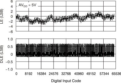
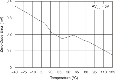
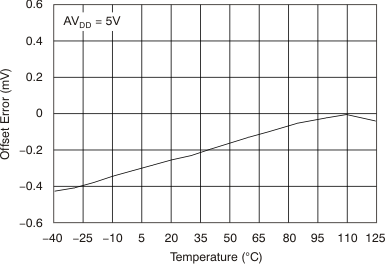
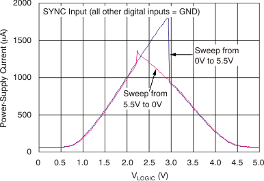
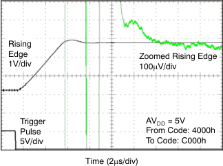
at TA = 25°C, AVDD = 5 V, and DAC loaded with mid-scale code, unless otherwise noted.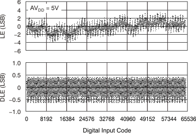


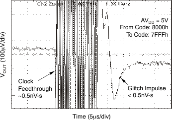
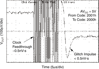
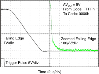
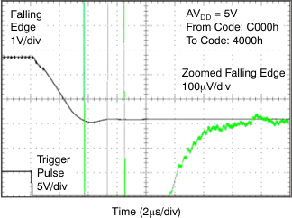
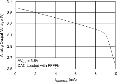
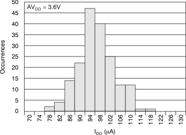
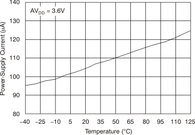
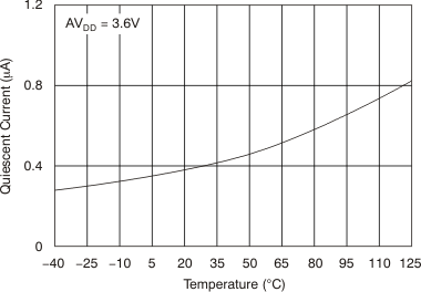
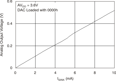
7.8.2 Typical Characteristics: AVDD = 3.6 V
at TA = 25°C, and AVDD = 3.6 V, unless otherwise noted.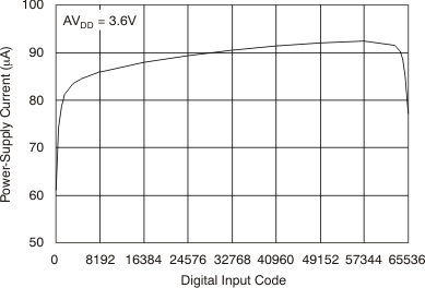
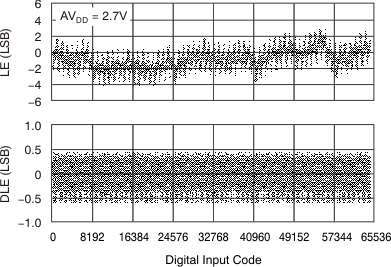
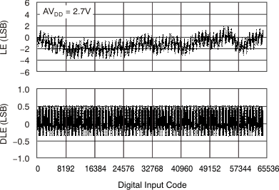
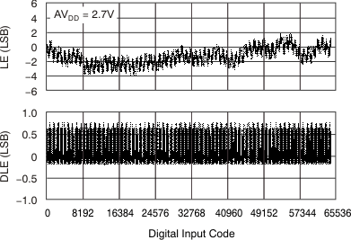
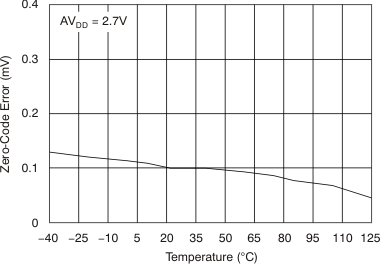
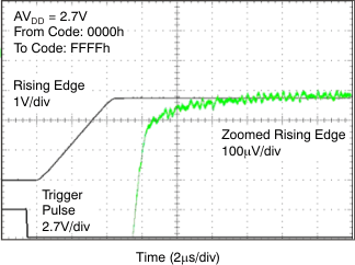
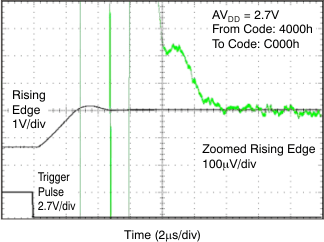
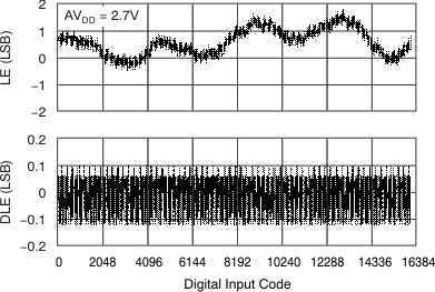
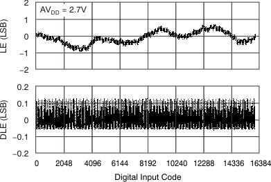
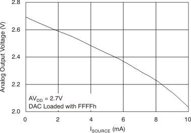
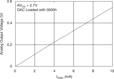
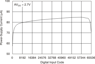
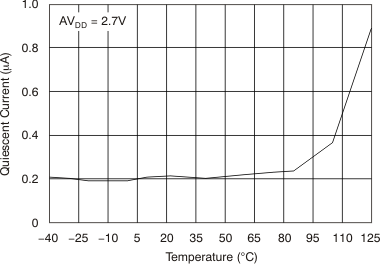
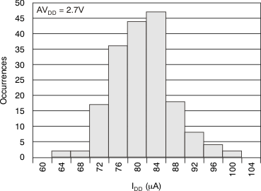
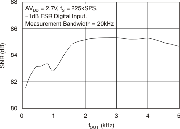
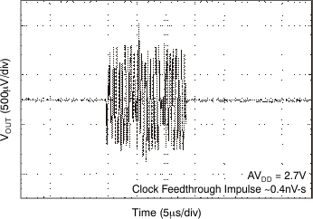
7.8.3 Typical Characteristics: AVDD = 2.7 V
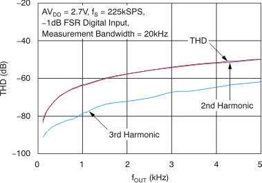
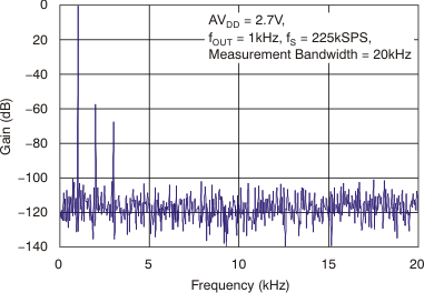
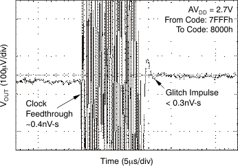
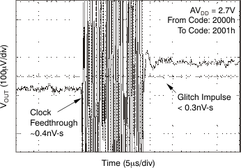
at TA = 25°C, and AVDD = 2.7 V, unless otherwise noted.