SBAS442D august 2008 – august 2023 DAC5311 , DAC6311 , DAC7311
PRODUCTION DATA
- 1
- 1 Features
- 2 Applications
- 3 Description
- 4 Revision History
- 5 Device Comparison
- 6 Pin Configuration and Functions
-
7 Specifications
- 7.1 Absolute Maximum Ratings
- 7.2 ESD Ratings
- 7.3 Recommended Operating Conditions
- 7.4 Thermal Information
- 7.5 Electrical Characteristics
- 7.6 Timing Requirements
- 7.7 Timing Diagrams
- 7.8 Typical Characteristics: AVDD = 5 V
- 7.9 Typical Characteristics: AVDD = 3.6 V
- 7.10 Typical Characteristics: AVDD = 2.7 V
- 8 Detailed Description
- 9 Application and Implementation
- 10Device and Documentation Support
- 11Mechanical, Packaging, and Orderable Information
8.4.1 Power-Down Modes
The DACx311 contain four separate modes of operation. These modes are programmable by setting two bits (PD1 and PD0) in the control register. Table 8-1 shows how the state of the bits corresponds to the mode of operation of the device.
| PD1 | PD0 | OPERATING MODE |
|---|---|---|
| NORMAL MODE | ||
| 0 | 0 | Normal Operation |
| POWER-DOWN MODES | ||
| 0 | 1 | Output 1 kΩ to GND |
| 1 | 0 | Output 100 kΩ to GND |
| 1 | 1 | High-Z |
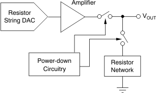
When both bits are set to 0, the device works normally with a standard power consumption of typically 80 μA at 2 V. However, for the three power-down modes, the typical supply current falls to 0.5 μA at 5 V, 0.4 μA at 3 V, and 0.1 μA at 2 V. Not only does the supply current fall, but the output stage is also internally switched from the output of the amplifier to a resistor network of known values. The advantage of this architecture is that the output impedance of the part is known while the part is in power-down mode. There are three different options: the output is connected internally to GND either through a 1-kΩ resistor or a 100-kΩ resistor, or is left open-circuited (High-Z). Figure 8-3 illustrates the output stage.
 Figure 8-3 Output Stage During Power-Down
All linear circuitry is shut down when the power-down mode is activated. However, the contents of the DAC register are unaffected when in power-down. The time to exit power-down is typically 50 μs for AVDD = 5 V and AVDD = 3 V.