SBAS444D May   2009  – January 2018 ADS1113 , ADS1114 , ADS1115

PRODUCTION DATA.  

  1. Features
  2. Applications
  3. Description
    1.     Device Images
      1.      Simplified Block Diagrams
  4. Revision History
  5. Device Comparison Table
  6. Pin Configuration and Functions
    1.     Pin Functions
  7. Specifications
    1. 7.1 Absolute Maximum Ratings
    2. 7.2 ESD Ratings
    3. 7.3 Recommended Operating Conditions
    4. 7.4 Thermal Information
    5. 7.5 Electrical Characteristics
    6. 7.6 Timing Requirements: I2C
    7. 7.7 Typical Characteristics
  8. Parameter Measurement Information
    1. 8.1 Noise Performance
  9. Detailed Description
    1. 9.1 Overview
    2. 9.2 Functional Block Diagrams
    3. 9.3 Feature Description
      1. 9.3.1 Multiplexer
      2. 9.3.2 Analog Inputs
      3. 9.3.3 Full-Scale Range (FSR) and LSB Size
      4. 9.3.4 Voltage Reference
      5. 9.3.5 Oscillator
      6. 9.3.6 Output Data Rate and Conversion Time
      7. 9.3.7 Digital Comparator (ADS1114 and ADS1115 Only)
      8. 9.3.8 Conversion Ready Pin (ADS1114 and ADS1115 Only)
      9. 9.3.9 SMbus Alert Response
    4. 9.4 Device Functional Modes
      1. 9.4.1 Reset and Power-Up
      2. 9.4.2 Operating Modes
        1. 9.4.2.1 Single-Shot Mode
        2. 9.4.2.2 Continuous-Conversion Mode
      3. 9.4.3 Duty Cycling For Low Power
    5. 9.5 Programming
      1. 9.5.1 I2C Interface
        1. 9.5.1.1 I2C Address Selection
        2. 9.5.1.2 I2C General Call
        3. 9.5.1.3 I2C Speed Modes
      2. 9.5.2 Slave Mode Operations
        1. 9.5.2.1 Receive Mode
        2. 9.5.2.2 Transmit Mode
      3. 9.5.3 Writing To and Reading From the Registers
      4. 9.5.4 Data Format
    6. 9.6 Register Map
      1. 9.6.1 Address Pointer Register (address = N/A) [reset = N/A]
        1. Table 6. Address Pointer Register Field Descriptions
      2. 9.6.2 Conversion Register (P[1:0] = 0h) [reset = 0000h]
        1. Table 7. Conversion Register Field Descriptions
      3. 9.6.3 Config Register (P[1:0] = 1h) [reset = 8583h]
        1. Table 8. Config Register Field Descriptions
      4. 9.6.4 Lo_thresh (P[1:0] = 2h) [reset = 8000h] and Hi_thresh (P[1:0] = 3h) [reset = 7FFFh] Registers
        1. Table 9. Lo_thresh and Hi_thresh Register Field Descriptions
  10. 10Application and Implementation
    1. 10.1 Application Information
      1. 10.1.1 Basic Connections
      2. 10.1.2 Single-Ended Inputs
      3. 10.1.3 Input Protection
      4. 10.1.4 Unused Inputs and Outputs
      5. 10.1.5 Analog Input Filtering
      6. 10.1.6 Connecting Multiple Devices
      7. 10.1.7 Quickstart Guide
    2. 10.2 Typical Application
      1. 10.2.1 Design Requirements
      2. 10.2.2 Detailed Design Procedure
        1. 10.2.2.1 Shunt Resistor Considerations
        2. 10.2.2.2 Operational Amplifier Considerations
        3. 10.2.2.3 ADC Input Common-Mode Considerations
        4. 10.2.2.4 Resistor (R1, R2, R3, R4) Considerations
        5. 10.2.2.5 Noise and Input Impedance Considerations
        6. 10.2.2.6 First-order RC Filter Considerations
        7. 10.2.2.7 Circuit Implementation
        8. 10.2.2.8 Results Summary
      3. 10.2.3 Application Curves
  11. 11Power Supply Recommendations
    1. 11.1 Power-Supply Sequencing
    2. 11.2 Power-Supply Decoupling
  12. 12Layout
    1. 12.1 Layout Guidelines
    2. 12.2 Layout Example
  13. 13Device and Documentation Support
    1. 13.1 Documentation Support
      1. 13.1.1 Related Documentation
    2. 13.2 Related Links
    3. 13.3 Receiving Notification of Documentation Updates
    4. 13.4 Community Resources
    5. 13.5 Trademarks
    6. 13.6 Electrostatic Discharge Caution
    7. 13.7 Glossary
  14. 14Mechanical, Packaging, and Orderable Information

Typical Application

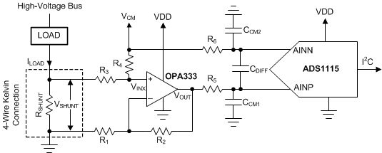
Shunt-based, current-measurement solutions are widely used to monitor load currents. Low-side, current-shunt measurements are independent of the bus voltage because the shunt common-mode voltage is near ground. Figure 44 shows an example circuit for a bidirectional, low-side, current-shunt measurement system. The load current is determined by measuring the voltage across the shunt resistor that is amplified and level-shifted by a low-drift operational amplifier, OPA333. The OPA333 output voltage is digitized with ADS1115 and sent to the microcontroller using the I2C interface. This circuit is capable of measuring bidirectional currents flowing through the shunt resistor with great accuracy and precision.
ADS1113 ADS1114 ADS1115 typapp_lowshunt_wrt2p5V_V2_generic_sbas444.gifFigure 44. Low-Side Current Shunt Monitoring